Pin description – Rainbow Electronics MAX887 User Manual
Page 7

MAX887
100% Duty Cycle, Low-Noise,
Step-Down, PWM DC-DC Converter
_______________________________________________________________________________________
7
______________________________________________________________Pin Description
NAME
FUNCTION
1
SHDN
Shutdown, Active-Low, Logic-Level Input. Connect
SHDN to V+ for normal operation.
2
FB
Feedback Input. Connect FB to a resistor voltage divider between the output and GND.
PIN
3
REF
Reference Bypass Output. Connect a 0.047µF capacitor to GND very close to the MAX887, within 0.2 in. (5mm).
4
VL
3.3V Internal Logic Regulator Output. Bypass VL to GND with a 2.2µF capacitor very close to the MAX887,
within 0.2 in. (5mm).
8
V+
Supply-Voltage Input. 3.5V min to 11V max. Bypass V+ to GND with a 0.33µF and large-value electrolytic
capacitor in parallel. These capacitors must be as close to the V+ and GND pins as possible. Place the
0.33µF capacitor within 0.2 in. (5mm) of the MAX887.
7
LX
Inductor Connection to the drain of an internal P-channel MOSFET
6
SYNC
Oscillator Synchronization and PWM Control Input. SYNC is a logic-level input. Tie SYNC to VL for internal
300kHz PWM operation at all loads. The oscillator synchronizes to the negative edge of an external clock
between 10kHz and 400kHz. The MAX887 operates in PWM mode when SYNC is clocked. Tying SYNC to
GND allows a reduced supply-current mode at light loads.
5
GND
Ground
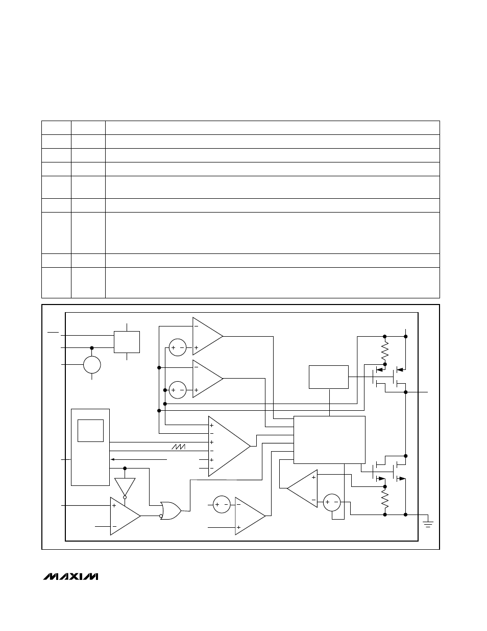
PFM CURRENT COMPARATOR
LEVEL
SHIFTER
CONTROL &
DRIVER LOGIC
SLOPE COMPENSATION
FROM CONTROL LOGIC
PWM
COMPARATOR
NEGLIM
COMPARATOR
0mV in PFM
ADJ. IN PWM
GND
0.1X
SENSE FET
SENSE FET
1
Ω
LX
V+
0.1X
1
Ω
PWM
REF
FB
SYNC
PFM
COMPARATOR
OVERVOLTAGE
COMPARATOR
PWM ON
SIGNAL
50mV
FB
REF
REF
FB
25mV
100mV
RAMP
GEN
SYNC
CELL
ILIM COMPARATOR
REF
VL
V+
GND
REF
GND
SHDN
VL
Figure 1. Simplified Functional Block Diagram
