Capacitor selection, Power dissipation, Layout considerations – Rainbow Electronics MAX1595 User Manual
Page 5
MAX1595
Regulated 3.3V/5.0V Step-Up/Step-Down
Charge Pump
_______________________________________________________________________________________
5
exceeds the available battery voltage, the use of a
charge pump such as the MAX1595 provides high effi-
ciency, small size, and constant light output with chang-
ing battery voltages. If the output is used only to light
LEDs, the output capacitor can be greatly reduced. The
frequency modulation of the LED intensity is not dis-
cernible to the human eye, and the smaller capacitor
saves both size and cost.
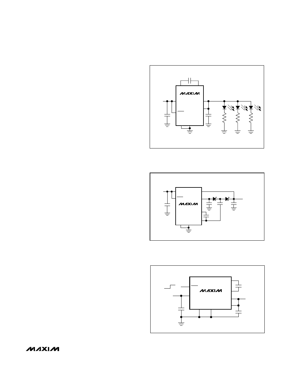
Adding two Schottky diodes and two capacitors imple-
ments a tripler and allows the MAX1595_ _ _50 to regu-
late a current of 75mA with a supply voltage as low as
2.3V (Figure 3).
Capacitor Selection
The MAX1595 requires only three external capacitors
(Figure 4). Their values are closely linked to the output
current capacity, oscillator frequency, output noise con-
tent, and mode of operation.
Generally, the transfer capacitor (C
X
) will be the smallest,
and the input capacitor (C
IN
) is twice as large as C
X
.
Higher switching frequencies allow the use of the smaller
C
X
and C
IN
. The output capacitor (C
OUT
) can be any-
where from 5-times to 50-times larger than C
X
. Table 1
shows recommended capacitor values.
In addition, the following equation approximates output
ripple:
V
RIPPLE
≅ I
OUT
/ (2 x f
OSC
x C
OUT
)
Table 2 lists the manufacturers of recommended capaci-
tors. Ceramic capacitors will provide the lowest ripple
due to their typically lower ESR.
Power Dissipation
The power dissipated in the MAX1595 depends on out-
put current and is accurately described by:
P
DISS
= I
OUT
(2V
IN
- V
OUT
)
P
DISS
must be less than that allowed by the package
rating.
Layout Considerations
All capacitors should be soldered in close proximity to
the IC. Connect ground and power ground through a
short, low-impedance trace. The input supply trace
should be as short as possible. Otherwise, an additional
input supply filter capacitor (tantalum or electrolytic) may
be required.
AOUT
IN
INPUT
2.3V
1
µF
SHDN
GND
PGND
OUT
MAX1595_ _ _50
0.22
µF
CXP
CXN
1
µF
OUTPUT
REGULATED 5V
75mA
1
µF
0.22
µF
OUT
IN
V
IN
C
OUT
=
0.47
µF
C
IN
= 1
µF
C
X
= 0.1
µF
SHDN
GND
CXP
CXN
PGND
AOUT
MAX1595_ _ _50
100
Ω
100
Ω
100
Ω
Figure 3. Regulated Voltage Tripler
Figure 2. White LED Bias Supply
C
X
0.22
µF
C
IN
1
µF
C
OUT
1
µF
OUT
CXN
CXP
SHDN
IN
OUT
7
4
6
3
2
8
ON
OFF
GND
5
PGND
AOUT
1
MAX1595
IN
Figure 4. Standard Operating Circuit