Rainbow Electronics MAX1011 User Manual
General description, Applications, Features
General Description
The MAX1011 is a 6-bit analog-to-digital converter
(ADC) that combines high-speed, low-power operation
with a user-selectable input range, an internal refer-
ence, and a clock oscillator. The ADC converts analog
signals into binary-coded digital outputs at sampling
rates up to 90Msps. The ability to directly interface with
baseband signals makes the MAX1011 ideal for use in
a wide range of communications and instrumentation
applications.
The MAX1011’s input amplifier features a true differential
input, a -0.5dB analog bandwidth of 55MHz, and a user-
programmable input full-scale range of 125mVp-p,
250mVp-p, or 500mVp-p. With an AC-coupled signal,
input offset is typically less than 1/4LSB. Dynamic per-
formance is 5.85 effective number of bits (ENOB) with a
20MHz analog input signal, or 5.7 ENOB with a 50MHz
signal.
The MAX1011 operates with +5V analog and +3.3V digi-
tal supplies for easy interfacing to +3.3V-logic-compatible
digital signal processors and microprocessors. It comes
in a 24-pin QSOP package.
Applications
IF Sampling Receivers
VSAT Receivers
Wide Local Area Networks (WLANs)
Instrumentation
Features
♦
High Sampling Rate: 90Msps
♦
Low Power Dissipation: 215mW
♦
Excellent Dynamic Performance:
5.85 ENOB with 20MHz Analog Input
5.7 ENOB with 50MHz Analog Input
♦
±1/4LSB INL and DNL (typ)
♦
±1/4LSB Input Offset (typ)
♦
Internal Bandgap Voltage Reference
♦
Internal Oscillator with Overdrive Capability
♦
55MHz (-0.5dB) Bandwidth Input Amplifier with
True Differential Input
♦
User-Selectable Full-Scale Range
(125mVp-p, 250mVp-p, or 500mVp-p)
♦
Single-Ended or Differential Input Drive
♦
Flexible, 3.3V, CMOS-Compatible Digital Outputs
MAX1011
Low-Power, 90Msps, 6-Bit ADC
________________________________________________________________
Maxim Integrated Products
1
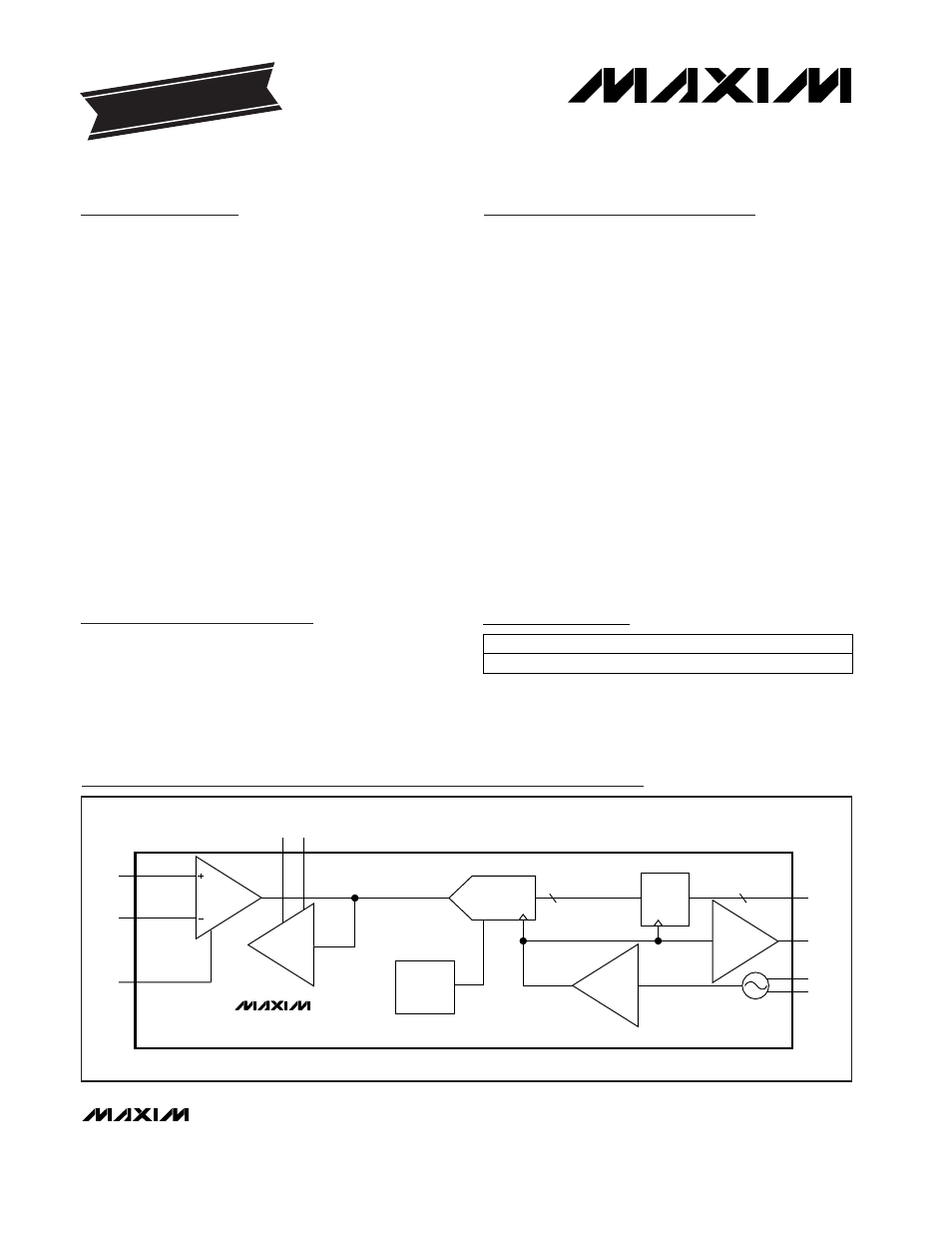
MAX1011
D0–D5
DCLK
TNK+
TNK-
INPUT
AMP
IN+
IN-
GAIN
DATA
BUFFER
6
ADC
VREF
BANDGAP
REFERENCE
OCC+
OCC-
6
OFFSET
CORREC-
TION
CLOCK
OUT
CLOCK
DRIVER
Functional Diagram
19-1335; Rev 0a; 2/98
PART
MAX1011CEG
0°C to +70°C
TEMP. RANGE
PIN-PACKAGE
24 QSOP
EVALUATION KIT
AVAILABLE
Pin Configuration appears at end of data sheet.
For free samples & the latest literature: http://www.maxim-ic.com, or phone 1-800-998-8800
For small orders, phone 408-737-7600 ext. 3468.
Ordering Information