Typical operating characteristics (continued), Pin description – Rainbow Electronics MAX662A User Manual
Page 3
MAX662A
+12V, 30mA Flash Memory
Programming Supply
_______________________________________________________________________________________
3
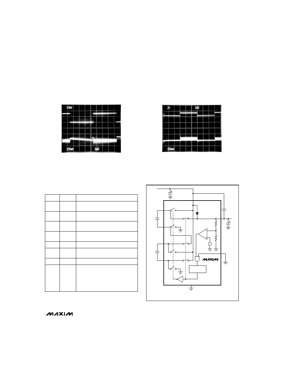
LOAD-TRANSIENT RESPONSE
A: OUTPUT CURRENT, 20mA/div, I
OUT
= 0mA to 30mA
B: OUTPUT VOLTAGE RIPPLE, 100mV/div, V
CC
= 5.0V
1ms/div
A
B
0mA
_____________________________Typical Operating Characteristics (continued)
(Circuit of Figure 3a, T
A
= +25°C, unless otherwise noted.)
LINE-TRANSIENT RESPONSE
A: SUPPLY VOLTAGE, 2V/div, V
CC
= 4.5V to 5.5V, I
OUT
= 30mA
B: OUTPUT VOLTAGE RIPPLE, 200mV/div
1ms/div
A
B
0V
0V
_____________________Pin Description
NAME
FUNCTION
1
C1-
Negative terminal for the first charge-
pump capacitor
PIN
2
C1+
Positive terminal for the first charge-
pump capacitor
4
C2+
Positive terminal for the second
charge-pump capacitor
3
C2-
Negative terminal for the second
charge-pump capacitor
7
GND
Ground
6
V
OUT
+12V Output Voltage. V
OUT
= V
CC
when in shutdown mode.
5
V
CC
Supply Voltage
8
Active-high CMOS-logic level
Shutdown Input. SHDN is internally
pulled up to V
CC
. Connect to GND for
normal operation. In shutdown mode,
the charge pumps are turned off and
V
OUT
= V
CC
.
SHDN
MAX662A
C1-
C1+
C2-
C2+
C4
4.7
µ
F
0.22
µ
F
0.22
µ
F
V
CC
V
CC
S1
S2
S1
S1
S1
S2
S2
GND
OSCILLATOR
VREF
R1
R2
SHDN
V
OUT
C5
4.7
µ
F
C3*
0.1
µ
F
+12V
SWITCH CLOSURES SHOWN FOR CHARGE PUMP IN THE TRANSFER MODE
* C3 NOT REQUIRED. FOR MAX662 ONLY.
ERROR
AMP
Figure 1. Block Diagram