Electrical characteristics – Rainbow Electronics MAX1685 User Manual
Page 4

MAX1684/MAX1685
Low-Noise, 14V Input, 1A, PWM
Step-Down Converters
4
_______________________________________________________________________________________
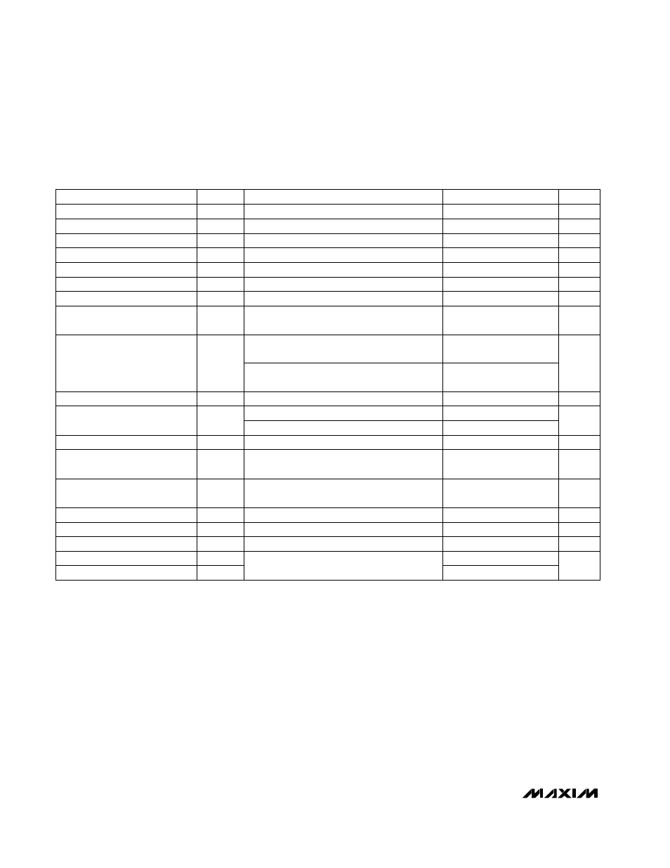
ELECTRICAL CHARACTERISTICS
(V
IN
= V
SHDN
= 6V, STBY = SYNC/PWM = CVL, V
BOOT
= V
OUT
, FB = AGND, circuit of Figure 1, T
A
= -40°C to +85°C, unless other-
wise noted.) (Note 5)
Note 1: The output adjust range with BOOT connected to V
OUT
is V
REF
to 5.5V. Connect BOOT to AGND for V
OUT
> 5.5V.
Note 2: The quiescent power-consumption specifications include chip supply and gate-drive loss only. Divide these values by V
IN
(6V) to obtain quiescent currents. In normal and low-power modes, chip supply current dominates and quiescent power is
proportional to V
BOOT
(BOOT connected to OUT). In PWM mode, gate-drive loss dominates and quiescent power is propor-
tional to V
IN
✕
(V
IN
- V
CVH
). In addition, IR losses in power switches and external components typically increase PWM quies-
cent power consumption by 5mW to 10mW. Note that if the device is not bootstrapped, additional power is dissipated in the
CVL linear regulator.
Note 3: When the duty factor (V
OUT
/ V
IN
) is less than this value, the switching frequency decreases in PWM mode to maintain
regulation.
Note 4: Thermal shutdown is disabled in low-power mode (STBY = low) to reduce power consumption.
Note 5: Specifications to -40°C are guaranteed by design, not production tested.
CVL Undervoltage Lockout
Threshold
2.4
2.6
V
BOOT = AGND, CVL falling edge,
typical hysteresis is 40mV
Logic Input Low Voltage
V
IL
0.7
Logic Input High Voltage
V
IH
2
V
SHDN, STBY, SYNC/PWM
ILIM/SS Source Current
3.1
4.7
µA
V
ILIM/SS
= 1.4V
0.27
Normal mode, SYNC/PWM = low,
V
BOOT
= 3.3V (Note 2)
BOOT Switchover Threshold
2.35
2.65
V
BOOT falling edge, typical hysteresis is 0.1V
CVH with Respect to V
IN
-5.0
-4.1
V
I
CVH
= -1mA
CVL Regulator Output Voltage
2.7
3.15
V
V
IN
= 3V to 14V, BOOT = AGND,
I
CVL
= 0 to 5mA
Reference Output Voltage
1.232
1.268
V
I
REF
= 0
Oscillator Frequency
f
OSC
480
700
kHz
MAX1685
240
350
MAX1684
Shutdown Supply Current
6
µA
SHDN = low
Quiescent Power Consumption
2
mW
Current Limit in Low-Power
Mode
I
LIMLP
285
475
mA
STBY = low
Output Voltage (3.3V Mode)
V
OUT
3.280
3.382
V
PARAMETER
SYMBOL
MIN
MAX
UNITS
FB Input Current
I
FB
-50
50
nA
Output Adjust Range
V
REF
V
IN
V
Output Current Capability
1
A
Input Voltage Range
2.7
14
V
Output Feedback Voltage
V
FB
1.233
1.269
V
Current Limit in PWM Mode
I
LIM
1.2
2.3
A
CONDITIONS
V
FB
= 1.4V
BOOT = AGND (Note 1)
V
IN
= 6V to 14V
FB = AGND, I
LOAD
= 0 to 1A
V
FB
= V
OUT
, I
LOAD
= 0 to 1A
Low-power mode, STBY = low,
V
BOOT
= 3.3V (Note 2)
