Max749 digitally adjustable lcd bias supply, Chip topography – Rainbow Electronics MAX749 User Manual
Page 11
Capacitors
Output Filter Capacitor
A 22µF, 30V surface-mount (SMT) tantalum output filter
capacitor typically maintains 100mVp-p output ripple
when generating -24V at 40mA from a 5V input. Smaller
capacitors, down to 10µF, may be used for light loads
in applications that can tolerate higher output ripple.
Surface-mount capacitors are generally preferred
because they lack the inductance and resistance of the
leads of their through-hole equivalents.
Input Bypass Capacitor
A 22µF tantalum capacitor in parallel with a 0.1µF
ceramic normally provides sufficient bypassing.
Mount
the 0.1µF capacitor very close to the IC.
Larger
capacitors may be needed if the incoming supply has
high impedance. Less bypass capacitance is accept-
able if the circuit is run off a low-impedance supply.
Begin prototyping with a large bypass capacitor; when
the circuit is working, reduce the bypass to the smallest
value that gives good results. Although bench power
supplies have low impedance at DC, they often have
high impedance at the frequencies used by switching
DC-DC converters.
The effective series resistance (ESR) of both the
bypass and filter capacitors affects efficiency. Best per-
formance is obtained by doubling up on the filter
capacitors or using low-ESR types.
The smallest low-ESR SMT capacitors currently avail-
able are Sprague 595D series, which are about half the
size of competing products. Sanyo OS-CON organic
semiconductor through-hole capacitors also exhibit low
ESR, and are especially useful when operation below
0°C is required. Table 2 lists the phone numbers of
these and other manufacturers.
Compensation Capacitor
The high value of the feedback resistor makes the feed-
back loop susceptible to phase lag if parasitic capaci-
tance is present at the FB pin. To compensate for this, it
may be necessary to connect a capacitor, C
COMP
, in
parallel with R
FB
. Although C
COMP
is normally not
required, the value of C
COMP
depends upon the value
of R
FB
and on the individual circuit layout—typical val-
ues range from 0pF to 220pF.
PC Layout and Grounding
Due to high current levels and fast switching wave-
forms, proper PC board layout is essential. In particular,
keep all leads short, especially the lead connected to
the FB pin and those connecting Q1, L1, and D1
together.
Mount the R
FB
resistor very close to the IC.
Use a star ground configuration: Connect the ground
lead of the input bypass capacitor, the output capaci-
tor, and the inductor at a common point next to the
GND pin of the MAX749. Additionally, connect the posi-
tive lead of the input bypass capacitor as close as pos-
sible to the V+ pin of the IC.
MAX749
Digitally Adjustable LCD Bias Supply
______________________________________________________________________________________
11
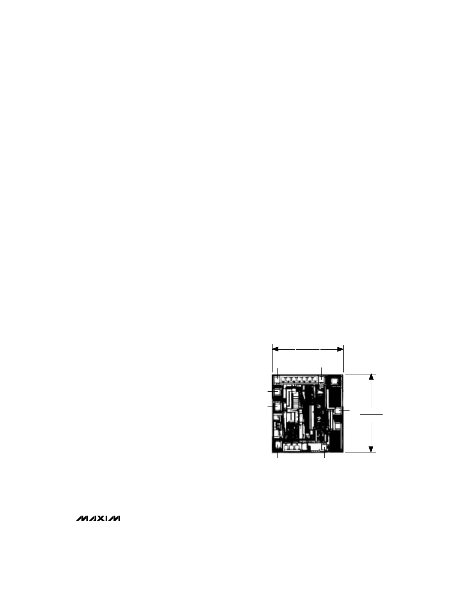
___________________Chip Topography
TRANSISTOR COUNT: 521;
SUBSTRATE CONNECTED TO GND.
ADJ
CTRL
0.070"
(0.1178mm)
0.808"
(0.2032mm)
FB
GND
V+
V+
CS
DLOW
DHI