Max864 dual-output charge pump with shutdown – Rainbow Electronics MAX864 User Manual
Page 2
MAX864
Dual-Output Charge Pump with Shutdown
2
_______________________________________________________________________________________
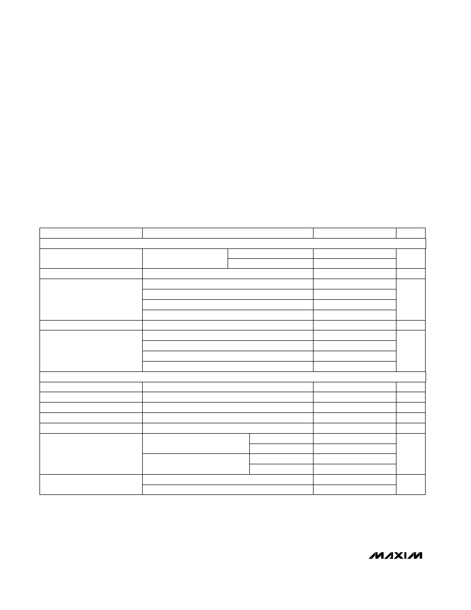
ABSOLUTE MAXIMUM RATINGS
ELECTRICAL CHARACTERISTICS (Note 1)
(V
IN
= 5V,
SHDN = V
IN
, circuit of Figure 1, T
A
= T
MIN
to T
MAX
, unless otherwise noted. Typical values are at T
A
= +25°C.)
Stresses beyond those listed under “Absolute Maximum Ratings” may cause permanent damage to the device. These are stress ratings only, and functional
operation of the device at these or any other conditions beyond those indicated in the operational sections of the specifications is not implied. Exposure to
absolute maximum rating conditions for extended periods may affect device reliability.
Note 1:
Measured using the capacitor values in Table 1. Capacitor ESR contributes approximately 10% of the output impedance
[ESR + 1 / (pump frequency x capacitance)].
V+ to GND ..............................................................-0.3V to +12V
SHDN, FC0, FC1 to GND .............................-0.3V to (V+ + 0.3V)
IN to GND ..............................................................-0.3V to +6.2V
V- to GND ...............................................................+0.3V to -12V
V- Output Current .............................................................100mA
V- Short Circuit to GND .................................................Indefinite
Operating Temperature Range
MAX864EEE......................................................-40°C to +85°C
Continuous Power Dissipation (T
A
= +70°C)
QSOP (derate 8.70mW/°C above +70°C) .....................696mW
Storage Temperature Range ............................ -65°C to +160°C
Lead Temperature (soldering, 10sec) .............................+300°C
Ω
60
V+ = 10V, I
V-
= 10mA (forced)
Output Resistance
(Note 1)
34
50
100
I
V+
= 10mA, I
V-
= 0mA
55
75
Ω
6
50
I
V-
= 10mA
V- to GND Shutdown Resistance
Ω
22
100
I
V+
= 10mA
V+ to IN Shutdown Resistance
µA
-1
1
SHDN, FC0 = FC1 = GND or IN
Logic Input Bias Current
V
3.5
2.8
SHDN, FC0, FC1
Logic Input High Voltage
V
2.2
1.0
SHDN, FC0, FC1
Logic Input Low Voltage
kHz
130
185
260
FC1 = FC0 = IN
Oscillator Frequency
V
6.0
R
LOAD
= 10k
Ω
Maximum Supply Voltage
V
2.00
Minimum Start-Up Voltage
70
100
140
FC1 = IN, FC0 = GND
24
33
48
FC1 = GND, FC0 = IN
5
7
10
FC1 = FC0 = GND
µA
0.1
1
FC1 = FC0 = IN or GND,
SHDN = GND
Shutdown Current
0.6
1.0
FC1 = FC0 = GND, f = 7kHz
2.4
3.65
FC1 = GND, FC0 = IN, f = 33kHz
7
11
FC1 = IN, FC0 = GND, f = 100kHz
mA
12
18
FC1 = FC0 = IN, f = 185kHz
Supply Current
UNITS
MIN
TYP
MAX
SYMBOL
PARAMETER
R
LOAD
= 10k
Ω
%
95
99
V-, R
L
=
∞
Voltage Conversion Efficiency
95
99
V+, R
L
=
∞
T
A
= T
MIN
to T
MAX
T
A
= +25°C
T
A
= +25°C
T
A
= T
MIN
to T
MAX
SUPPLY
INPUTS AND OUTPUTS
T
A
= +25°C
T
A
= T
MIN
to T
MAX
1.75
1.25