Electrical characteristics (continued) – Rainbow Electronics MAX1635 User Manual
Page 4
MAX1630–MAX1635
Multi-Output, Low-Noise Power-Supply
Controllers for Notebook Computers
4
_______________________________________________________________________________________
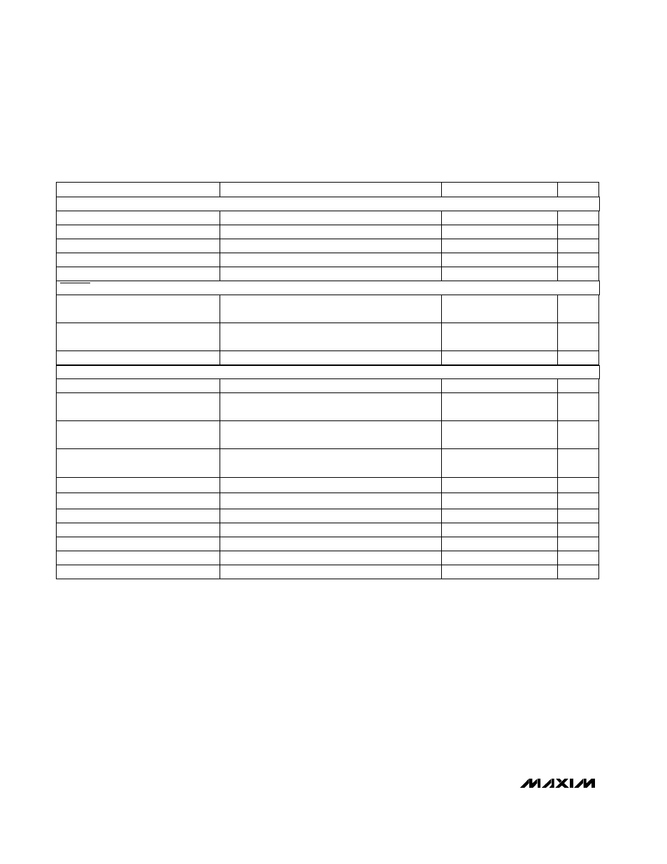
Note 1:
Each of the four digital soft-start levels is tested for functionality; the steps are typically in 20mV increments.
Note 2:
High duty-factor operation supports low input-to-output differential voltages, and is achieved at a lowered operating
frequency (see
Overload and Dropout Operation
section).
Note 3:
MAX1630/MAX1632/MAX1633/MAX1635 only.
Note 4:
Off mode for the 12V linear regulator occurs when the SMPS that has flyback feedback (V
DD
) steered to it is disabled. In
situations where the main outputs are being held up by external keep-alive supplies, turning off the 12OUT regulator pre-
vents a leakage path from the output-referred flyback winding, through the rectifier, and into V
DD
.
Note 5:
Since the reference uses VL as its supply, the reference’s V+ line-regulation error is insignificant.
ELECTRICAL CHARACTERISTICS (continued)
(V+ = 15V, both PWMs on, SYNC = VL, VL load = 0mA, REF load = 0mA, SKIP = 0V, T
A
= T
MIN
to T
MAX
, unless otherwise noted.
Typical values are at T
A
= +25°C.)
Typical hysteresis = +10°C
From each SMPS enabled, with respect to f
OSC
°C
150
clks
5000
6144
7000
With respect to unloaded output voltage
Output Undervoltage Lockout Time
Thermal Shutdown Threshold
With respect to f
OSC
Falling edge, CSL_ driven 2%
below RESET trip threshold
clks
27,000
32,000
37,000
µs
1.5
With respect to unloaded output voltage,
falling edge; typical hysteresis = 1%
RESET Propagation Delay
RESET Delay Time
%
-7
-5.5
-4
CONDITIONS
RESET Trip Threshold
RESET, I
SINK
= 4mA
RUN/ON3, SKIP, TIME/ON5 (SEQ = REF),
SHDN, STEER, SYNC, SEQ; V
PIN
= 0V or 3.3V
V
0.4
µA
±1
Input Leakage Current
Logic Output Low Voltage
CSL_ driven 2% above overvoltage trip threshold
µs
FB3, FB5; SECFB = 2.6V
1.5
Overvoltage-Fault Propagation Delay
nA
1
50
With respect to unloaded output voltage
%
60
70
80
Feedback Input Leakage Current
Output Undervoltage Threshold
%
4
7
10
Overvoltage Trip Threshold
RUN/ON3, SKIP, TIME/ON5 (SEQ = REF),
SHDN, STEER, SYNC
RUN/ON3, SKIP, TIME/ON5 (SEQ = REF),
SHDN, STEER, SYNC
V
2.4
V
0.6
Logic Input Low Voltage
Logic Input High Voltage
UNITS
MIN
TYP
MAX
PARAMETER
High or low
DL3, DH3, DL5, DH5; forced to 2V
Ω
1.5
7
A
1
Gate Driver Sink/Source Current
Gate Driver On-Resistance
RESET = 3.5V
mA
1
Logic Output High Current
TIME/ON5 = 0V, SEQ = 0V or VL
SEQ = 0V or VL
µA
2.5
3
3.5
V
2.4
2.6
TIME/ON5 Input Trip Level
TIME/ON5 Source Current
TIME/ON5; RUN/ON3 = 0V, SEQ = 0V or VL
Ω
15
80
TIME/ON5 On-Resistance
FAULT DETECTION
(MAX1630/MAX1631/MAX1632)
INPUTS AND OUTPUTS
RESET