Pin description – Rainbow Electronics MAX1865 User Manual
Page 9
MAX1864/MAX1865
xDSL/Cable Modem Triple/Quintuple Output
Power Supplies
_______________________________________________________________________________________
9
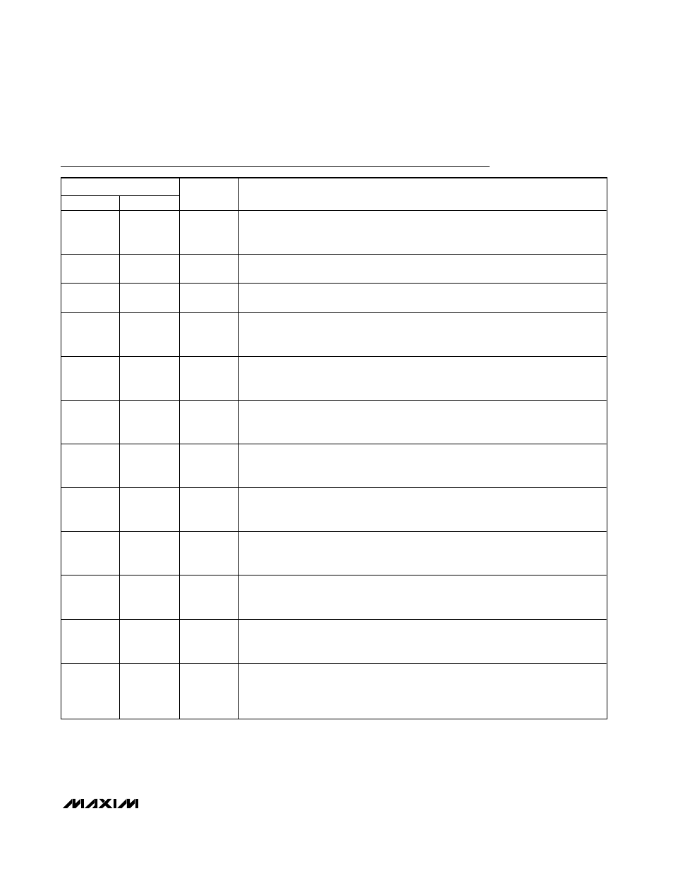
Pin Description
PIN
MAX1864
MAX1865
NAME
FUNCTION
1
1
POK
Open-Drain Power-Good Output. POK is low when the output voltage is more than
10% below the regulation point. POK is high impedance when the output is in
regulation. Connect a resistor between POK and VL for logic-level voltages.
2
2
COMP
Compensation Pin. Connect a series RC to GND to compensate the control loop.
Typical values are 47k
Ω and 8.2nF.
3
3
OUT
Regulated Output Voltage High-Impedance Sense Input. Internally connected to a
resistive-divider and negative gain block (MAX1865).
4
4
FB
Dual-Mode Switching-Regulator Feedback Input. Connect to GND for the preset 3.3V
output. Connect to a resistive-divider from output to FB to GND to adjust the output
voltage between 1.236V and 0.8
✕
V
IN
. The feedback set point is 1.236V.
5
5
B2
Open-Drain Output PNP Transistor Driver (Regulator #2). Internally connected to the
drain of a DMOS. B2 connects to the base of an external PNP pass transistor to form a
positive linear regulator.
6
6
FB2
Analog Gain-Block Feedback Input (Regulator #2). Connect to a resistive-divider
between the positive linear regulator’s output and GND to adjust the output voltage.
The feedback set point is 1.24V.
7
7
B3
Open-Drain Output PNP Transistor Driver (Regulator #3). Internally connected to the
drain of a DMOS. B3 connects to the base of an external PNP pass transistor to form a
positive linear regulator.
8
8
FB3
Analog Gain-Block Feedback Input (Regulator #3). Connect to a resistive-divider
between the positive linear regulator’s output and GND to adjust the output voltage.
The feedback set point is 1.24V.
—
9
B4
Open-Drain Output PNP Transistor Driver (Regulator #4). Internally connected to the
drain of a DMOS. B4 connects to the base of an external PNP pass transistor to form a
positive linear regulator.
—
10
FB4
Analog Gain-Block Feedback Input (Regulator #4). Connect to a resistive-divider
between the positive linear regulator’s output and GND to adjust the output voltage.
The feedback set point is 1.24V.
—
11
B5
Open-Drain Output NPN Transistor Driver (Regulator #5). Internally connected to the
drain of a P-channel MOSFET. B5 connects to the base of an external NPN pass
transistor to form a negative linear regulator.
—
12
FB5
Analog Gain-Block Feedback Input (Regulator #5). Connect to a resistive-divider
between the negative linear regulator’s output and a positive reference voltage,
typically one of the positive linear regulator outputs, to adjust the output voltage. The
feedback set point is at GND.