Apr9301, Integrated circuits inc – Rainbow Electronics APR9301 User Manual
Page 7
INTEGRATED CIRCUITS INC.
-
APR9301
http://www.aplusinc.com.tw
Page / 10 VER2.1
7
Table 4 Analog Characteristics ( Note 1 )
Item
Symbol
Condition
Mim Typ Max
Unit
MicIn Input Voltage
VMI
--
--
--
20
mVp-p
MicIn
Input
Resistance
RMI
--
-- 10 -- kΩ
MicIn Amp Gain (1)
GMIl
AGC≦2.2V
-- 24 -- dB
MicIn Amp Gain (2)
GMI2
AGC≧3.OV
-- -45 -15 dB
AnaIn Input Voltage
VANI
--
--
--
50
mVp-p
AnaIn
Input
Resistance RANI
--
-- 10 -- kΩ
AnaIn Amp Gain
GANI
Analn to SP+/-
--
22
--
dB
AGC
Output
Resistance RAGC
--
-- 1 -- kΩ
SP+/- Output Power
Psp
Rsp+/- = 16Ω
-- 12.2 -- mW
Voltage Amplitude Across SP+/-
Vsp
Rsp+/-≧16Ω
-- 1.25 -- Vp-p
Total Harmonic Distortion
THD
@ 1kHz & 20mVp-p input
1 %
Note 1: Typical Values: VCCD = VCCA = 5V; VSSD = VSSA = 0V; TA = 25℃
Note 2: Except pins 23 and 27 which have internal pull-up resistors.
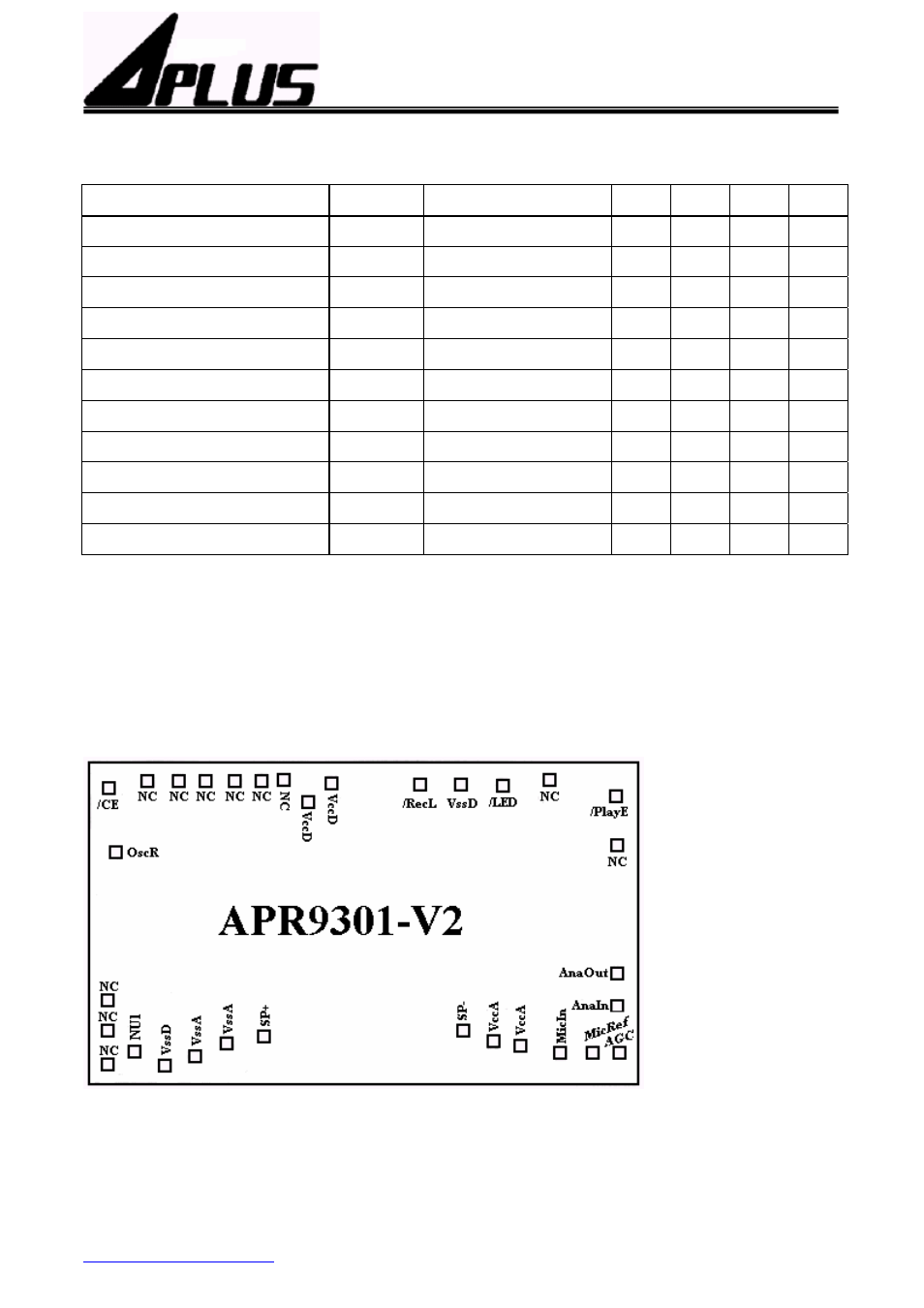
Bonding Pad Diagram & Description of Bonding Pad Coordinates :
Figure 5 APR9301 Die Bonding Pad Diagram
Notes:
Die diagram is with
respect to die center(um)
Die Dimensions:
X=214± 1 mils(5500um)
Y=144± 1 mils(3750um)
Die Thickness:
13.8± 1.0 mils
(350± 25um)
Pad Opening:
4.3mils
110um
*
Connect substrate
to Ground.