Apexx08 series – Rainbow Electronics APExx08 User Manual
Page 4
APExx08 Series
Rev 1.5 2004/4/20
3
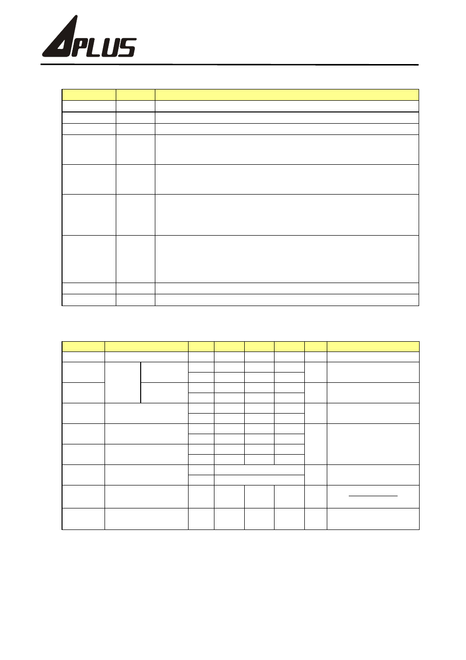
3.0 Pin Description
Pad Name
Pin Attr.
Description
PWM2/Cout
O
PWM2 output, or Current Output of Audio.
PWM1
O PWM1
output.
Vdd1~2
Power
Power supply during operation.
PRA0~3
I/O
I/O port can be programmed to input/output individually.
Input type with weak pull-low or fix-input-floating capability.
Buffer Output type.
PRB0, PRB2
I/O
I/O port can be configured to input/output individually.
Input type with weak pull-low or fix-input-floating capability.
Buffer Output type.
PRB1 / IR
I/O
I/O port can be configured to input/output individually.
Input type with weak pull-low or fix-input-floating capability.
Buffer Output type.
Mask option selected as an IR Carrier Output with 38k / 56kHz
PRB3 / Reset
I/O
I/O port can be configured to input/output individually.
Input type with weak pull-low or fix-input-floating capability.
Buffer Output type.
Mask option selected as an external RESET pin with weak pull-low
capability.
OSC
I
RM mode Oscillator input
GND1~2
Power
Ground Potential
4.0 DC Characteristics
Symbol
Parameter
Vdd
Min.
Typ.
Max.
Unit
Condition
Vdd Operating voltage 2.4 3 5.5 V depending on Freq.
3 1
Isb Standby
4.5
1
uA
4MHz, RM,
in HALT Mode
3 1
Iop
Supply
current
Operating
4.5 2.5
mA
4MHz, RM,
IO Floating
3 4
Iih
Input current
(Internal pull low)
4.5 10
uA
Input ports with weak
pull-low
3 -4
Ioh Output-high
current
4.5 -10
3 8.5
Iol Output-low
current
4.5 17.5
mA
4MHz, RM
(IO ports)
3
0.8 ~ 4.8
Cout
DAC output current
(8-level option)
4.5
0.9 ~ 6.5
mA
4MHz, RM
(Full scale)
dF/F Frequency
stability -5 5 %
Fosc(3v- 2.4v)
Fosc (3v)
dF/F
Fosc lot variation
-10
10
%
Vdd=3V, Rosc=430k,
4MHz