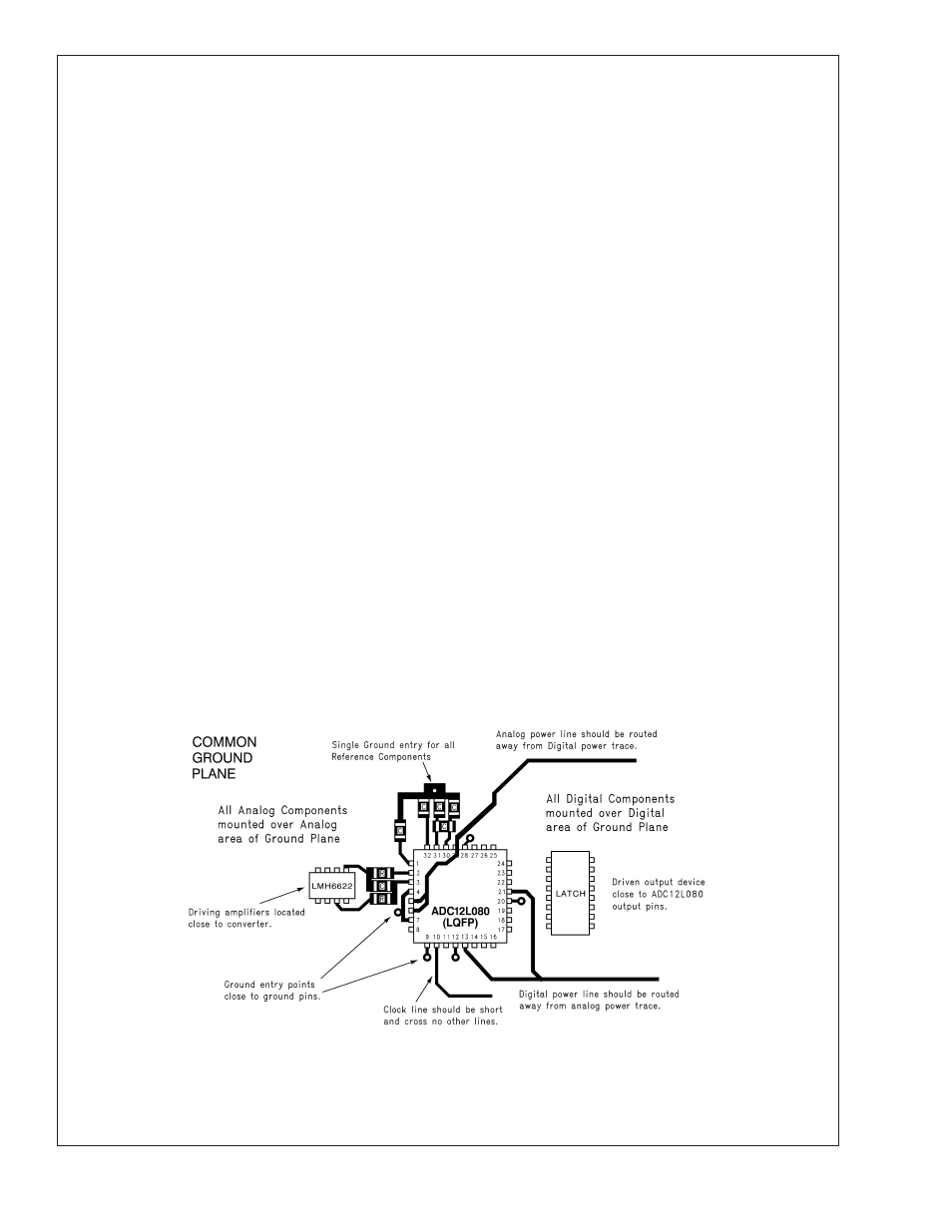
0 power supply considerations, 0 layout and grounding, Figure 7. example of a suitable layout – Rainbow Electronics ADC12L080 User Manual
Page 21: Applications information

Applications Information
(Continued)
5.0 POWER SUPPLY CONSIDERATIONS
The power supply pins should be bypassed with a 10 µF
capacitor and with a 0.1 µF low ESL ceramic chip capacitor
within 3 millimeters of each power pin.
As is the case with all high-speed converters, the
ADC12L080 is sensitive to power supply noise. Accordingly,
the noise on the analog supply pin should be kept below 100
mV
P-P
.
No pin should ever have a voltage on it that is in excess of
the supply voltages, not even on a transient basis. Be espe-
cially careful of this during turn on and turn off of power.
The V
DR
pin provides power for the output drivers and may
be operated from a supply in the range of 1.8V to V
D
. This
can simplify interfacing to devices and systems operating
with supplies less than V
D
. DO NOT operate the V
DR
pin at
a voltage higher than V
D
.
6.0 LAYOUT AND GROUNDING
Proper grounding and proper routing of all signals are es-
sential to ensure accurate conversion. Maintaining separate
analog and digital areas of the board, with the ADC12L080
between these areas, is required to achieve specified per-
formance.
The ground return for the data outputs (DR GND) carries the
ground current for the output drivers. The output current can
exhibit high transients that could add noise to the conversion
process. To prevent this from happening, the DR GND pins
should NOT be connected to system ground in close prox-
imity to any of the ADC12L080’s other ground pins.
Capacitive coupling between the typically noisy digital cir-
cuitry and the sensitive analog circuitry can lead to poor
performance. The solution is to keep the analog circuitry
separated from the digital circuitry, and to keep the clock line
as short as possible.
Digital circuits create substantial supply and ground current
transients. The logic noise thus generated could have sig-
nificant impact upon system noise performance. The best
logic family to use in systems with A/D converters is one
which employs non-saturating transistor designs, or has low
noise characteristics, such as the 74LS, 74HC(T) and
74AC(T)Q families. The worst noise generators are logic
families that draw the largest supply current transients dur-
ing clock or signal edges, like the 74F and the 74AC(T)
families.
The effects of the noise generated from the ADC output
switching can be minimized through the use of 100
Ω resis-
tors in series with each data output line. Locate these resis-
tors as close to the ADC output pins as possible.
Since digital switching transients are composed largely of
high frequency components, total ground plane copper
weight will have little effect upon the logic-generated noise.
This is because of the skin effect. Total surface area is more
important than is total ground plane volume.
Generally, analog and digital lines should cross each other at
90˚ to avoid crosstalk. To maximize accuracy in high speed,
high resolution systems, however, avoid crossing analog and
digital lines altogether. It is important to keep clock lines as
short as possible and isolated from ALL other lines, including
other digital lines. Even the generally accepted 90˚ crossing
should be avoided with the clock line as even a little coupling
can cause problems at high frequencies. This is because
other lines can introduce jitter into the clock line, which can
lead to degradation of SNR. Also, the high speed clock can
introduce noise into the analog chain.
Best performance at high frequencies and at high resolution
is obtained with a straight signal path. That is, the signal path
through all components should form a straight line wherever
possible.
Be especially careful with the layout of inductors. Mutual
inductance can change the characteristics of the circuit in
which they are used. Inductors should not be placed side by
side, even with just a small part of their bodies beside each
other.
The analog input should be isolated from noisy signal traces
to avoid coupling of spurious signals into the input. Any
external component (e.g., a filter capacitor) connected be-
20061016
FIGURE 7. Example of a Suitable Layout
ADC12L080
www.national.com
21
