7v to 5.5v), Timing diagrams – Rainbow Electronics DS1624 User Manual
Page 15
DS1624
15 of 16
AC ELECTRICAL CHARACTERISTICS
(-55°C to +125°C; V
DD
=2.7V to 5.5V)
PARAMETER
SYMBOL
MIN
TYP
MAX
UNITS
NOTES
Input Capacitance
C
I
5
pF
NOTES:
1. All voltages are referenced to ground.
2. I/O pins of fast mode devices must not obstruct the SDA and SCL lines if V
DD
is switched off.
3. I
CC
specified with SDA pin open.
4. I
CC
specified with V
CC
at 5.0V and SDA, SCL = 5.0V, 0
°
C to 70
°
C.
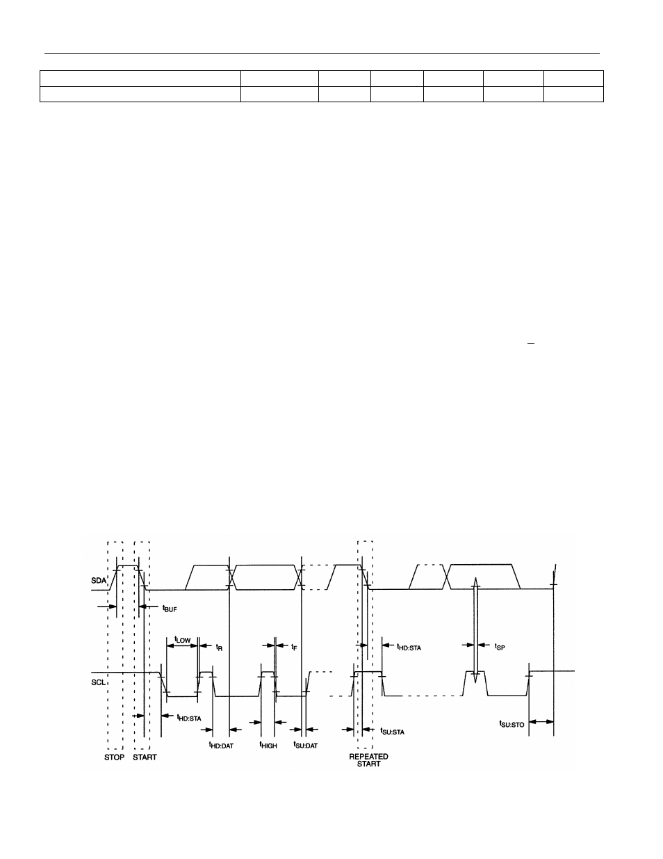
5. After this period, the first clock pulse is generated.
6. The maximum t
HD:DAT
has only to be met if the device does not stretch the LOW period (t
LOW
) of the
SCL signal.
7. A fast mode device can be used in a standard mode system, but the requirement t
SU:DAT
>250 ns must
then be met. This will automatically be the case if the device does not stretch the LOW period of the
SCL signal. If such a device does stretch the LOW period of the SCL signal, it must output the next
data bit to the SDA line t
RMAX
+t
SU:DAT
= 1000+250 = 1250 ns before the SCL line is released.
8. C
b
– total capacitance of one bus line in pF.
9. Writing to the nonvolatile memory should only take place in the 0°C to 70°C temperature range.
10. See Typical Curve for specification limits outside the 0°C to 70°C temperature range. Thermometer
error reflects sensor accuracy as tested during calibration.
TIMING DIAGRAMS