Electrical characteristics, Block diagram, 5 threshold voltage stb1 – Rainbow Electronics BD9731KV User Manual
Page 2: 5=2v, 1v vscp=0v, Iosink vstbh vstbl oscillating frequency stb pin control voltage, Circuit current at stand-by
Electrical characteristics (
Unless otherwise noted; Ta=25˚C, Vcc=6V, fosc=0.20MHz, STB1~5=3V)
Circuit current at stand-by
Ist
—
—
1.485
2.4
1.425
0.90
—
4.5
1.5
2.5
1.5
1.0
10
9.5
1.515
2.6
1.575
1.10
µA
mA
V
V
V
V
Icc
Vref
VREGA
Vsc1~5
Vtsc
Circuit current at operating
Output voltage
Output voltage REGA
CH1
~
5 threshold voltage
STB1
~
5=0V
Iref=–1mA
Ireg=–1mA
VSCP1
~
5=2V
~
1V
VSCP=0V
~
1.5V
Symbol
Min.
Max.
Unit
Conditions
Typ.
Parameter
Triangle wave oscillator
fosc1
0.179
Vcc–0.3
—
—
—
2.0
–0.3
0.20
Vcc–0.1
0.1
—
—
—
—
0.221
—
0.3
30
–30
—
0.3
MHz
V
V
mA
mA
V
V
VSATH
VSATL
I
OSOURCE
Iosink
VSTBH
VSTBL
Oscillating frequency
Output voltage 'H' at operating
Output voltage 'L' at operating
Maximum output source current
Maximum output sink current
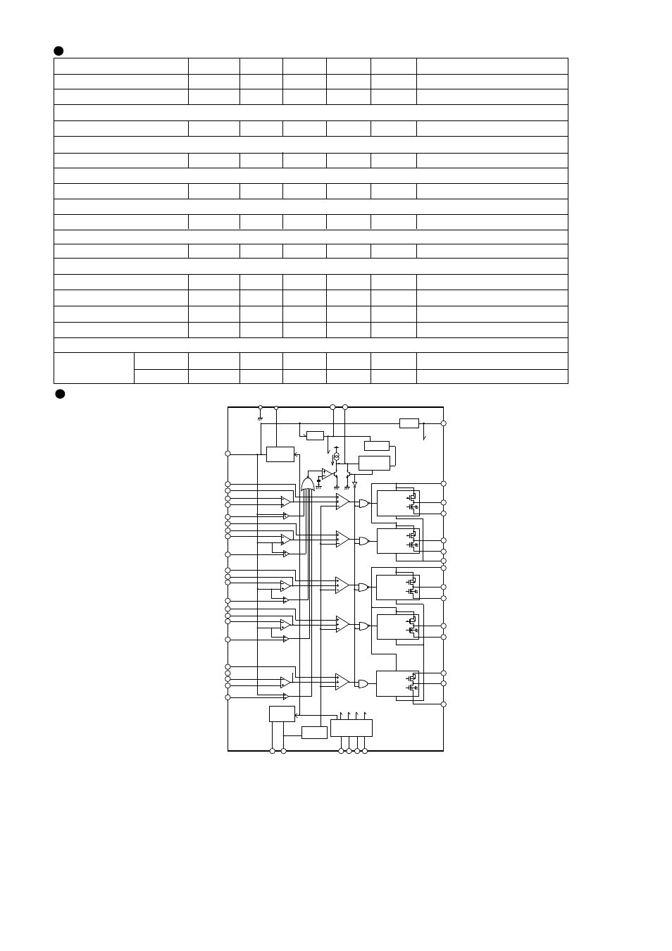
~ 5> STB pin Operating Non-operating RT=24k Ω, CT=220pF Io=10mA SCP pin detection circuit Block Diagram Pch DRIVER Pch DRIVER Pch DRIVER Nch DRIVER REG A VOLTAGE REFERENCE REG D U.V.L.O TIMER LATCH S Q R TRIANGLE FORM OSC OSC BUFFER ON/OFF LOGIC VREGD PVCC1 OUT1 RBIAS1 OUT2 RBIAS2 PGND1 OUT3 RBIAS3 OUT4 RBIAS4 RBIAS5 OUT5 PGND2 SCP5 S T B 5 S T B 4 S T B 23 S T B 1 C T R T NON5 INV5 FB5 DTC5 SCP4 INV4 FB4 DTC4 SCP3 INV3 FB3 DTC3 INV2 FB2 DTC2 SCP1 NON1 INV1 FB1 DTC1 VREF 30 .G N D 32 .V C C V R E G A S C P To Control To-Divers ERRAMP1 ERRAMP2 ERRAMP3 ERRAMP4 ERRAMP5 PWM PWM PWM PWM PWM SCP2 Block SCPcomp1 SCPcomp2 SCPcomp3 SCPcomp4 SCPcomp5 Pch DRIVER BD9731KV 34 43 41 39 38 37 26 25 19 20 14 15 31 29 33 3 2 1 4 5 44 8 7 6 9 10 13 12 11 27 28 48 47 46 45
control voltage
Io=–10mA
PVCC2
40
42
36
35
24
23
21
22
16
17
18