Special function registers, At89c55wd – Rainbow Electronics AT89C55WD User Manual
Page 6
6
AT89C55WD
1921B–MICRO–09/02
Special
Function
Registers
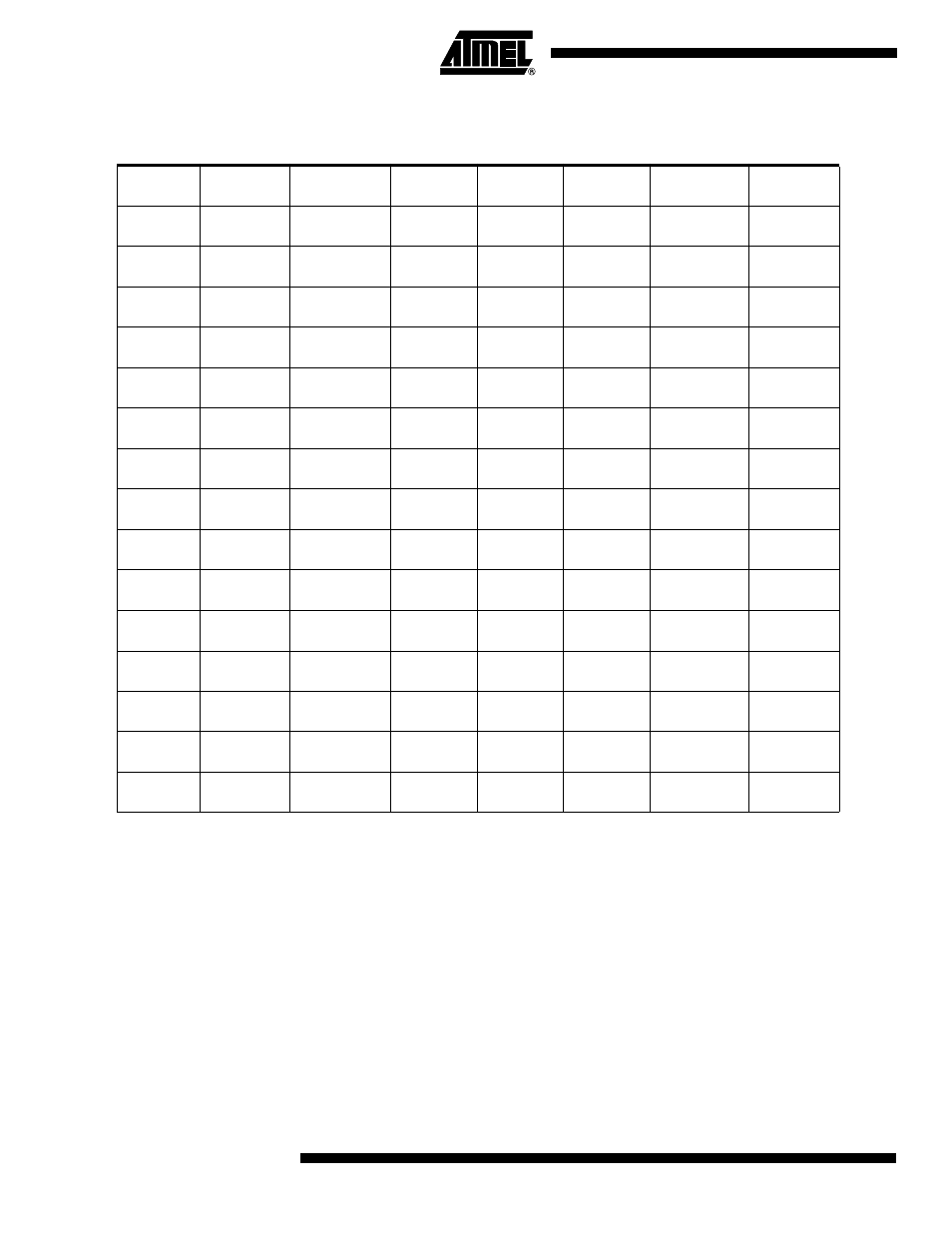
A map of the on-chip memory area called the Special Function Register (SFR) space is shown
in Table 1.
Note that not all of the addresses are occupied, and unoccupied addresses may not be imple-
mented on the chip. Read accesses to these addresses will in general return random data,
and write accesses will have an indeterminate effect.
User software should not write 1s to these unlisted locations, since they may be used in future
products to invoke new features. In that case, the reset or inactive values of the new bits will
always be 0.
Timer 2 Registers: Control and status bits are contained in registers T2CON (shown in Table
2) and T2MOD (shown in Table 2) for Timer 2. The register pair (RCAP2H, RCAP2L) are the
Capture/Reload registers for Timer 2 in 16-bit capture mode or 16-bit auto-reload mode.
Table 1. AT89C55WD SFR Map and Reset Values
0F8H
0FFH
0F0H
B
00000000
0F7H
0E8H
0EFH
0E0H
ACC
00000000
0E7H
0D8H
0DFH
0D0H
PSW
00000000
0D7H
0C8H
T2CON
00000000
T2MOD
XXXXXX00
RCAP2L
00000000
RCAP2H
00000000
TL2
00000000
TH2
00000000
0CFH
0C0H
0C7H
0B8H
IP
XX000000
0BFH
0B0H
P3
11111111
0B7H
0A8H
IE
0X000000
0AFH
0A0H
P2
11111111
AUXR1
XXXXXXX0
WDTRST
XXXXXXXX
0A7H
98H
SCON
00000000
SBUF
XXXXXXXX
9FH
90H
P1
11111111
97H
88H
TCON
00000000
TMOD
00000000
TL0
00000000
TL1
00000000
TH0
00000000
TH1
00000000
AUXR
XXX00XX0
8FH
80H
P0
11111111
SP
00000111
DP0L
00000000
DP0H
00000000
DP1L
00000000
DP1H
00000000
PCON
0XXX0000
87H