Regulator ics ba3932 – Rainbow Electronics BA3932 User Manual
Page 6
158
Regulator ICs
BA3932
Calculation of P
MAX
S
Power consumed by AUDIO 9V
P
1
= (V
CC
– 9.0V)
I1
S
Power consumed by MOTOR 14.7V
P
2
= (V
CC
– 14.7V)
I2
S
Power consumed by CD 8.0V
P
3
= (V
CC
– 8.0V)
I3
S
Power consumed by CD 5.0V
P
4
= (V
CC
– 5.0V)
I4
S
Power consumed by RADIO 5.0V
P
5
= (V
CC
– 5.0V)
I5
S
Power consumed by COM 5.0V
P
6
= (V
CC
– 5.0V)
I6
S
Power consumed internally by each circuit
P
7
= V
CC
circuit current
∗
I
1
= maximum output for AUDIO 9V
I
2
= maximum output for MOTOR 14.7V
I
3
= maximum output for CD 8.0V
I
4
= maximum output for CD 5.0V
I
5
= maximum output for RADIO 5.0V
I
6
= maximum output for COM 5.0V
F
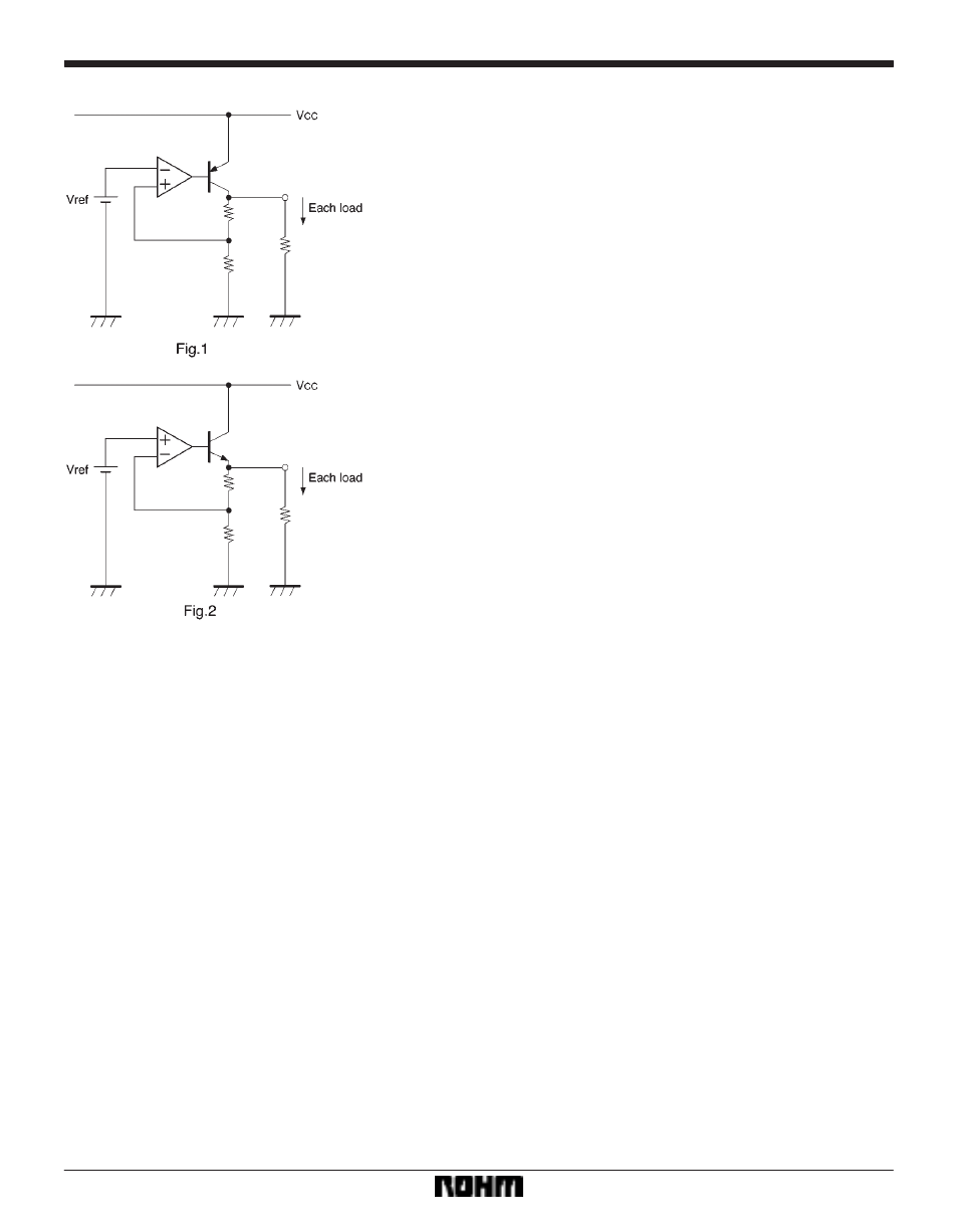
Operation notes
(1)
Operating power supply voltage
When operating within proper ranges of power supply
voltage and ambient temperature, most circuit functions
are guaranteed. Although the rated values of electrical
characteristics cannot be absolutely guaranteed, char-
acteristic values do not change drastically within the
proper ranges.
(2)
Power dissipation (Pd)
Refer to the heat reduction characteristics (Fig. 3) and
the rough estimation of IC power dissipation given on a
separate page. Make sure to use the IC within the allow-
able power dissipation with a sufficient margin.
(3)
Preventing oscillation at each output and installing
a ripple filter capacitor.
To stop oscillation of output, make sure to connect a ca-
pacitor between GND and each of the AUDIO 9V (pin 1),
RADIO (pin 4), COM (pin 5), CD 5V (pin 6), CD 8V (pin
7), and MOTOR 14.7V (pin 11) output pins. We recom-
mend using a tantalum electrolytic capacitor having a ca-
pacitance of 10
µ
F or greater (100
µ
F or greater for AU-
DIO 9V) with minimal temperature susceptibility. Also,
sudden deterioration of the AUDIO 9V ripple rejection
during a power drop can be prevented by connecting a
capacitor (220
µ
F or greater recommended) to the C pin
(pin 2).
(4)
Overcurrent protection circuit
An overcurrent protection circuit is installed on the AU-
DIO 9V (pin 1), RADIO (pin 4), COM (pin 5), CD 5V (pin
6), CD 8V (pin 7), and MOTOR 14.7V (pin 11) outputs,
based on the respective output current. This prevents IC
destruction by overcurrent, by limiting the current with a
curve shape of “7” in the voltage-current graph. The IC
is designed with margins so that current flow will be re-
stricted and latching will be prevented even if a large cur-
rent suddenly flows through a large capacitor. Note that
these protection circuits are only good for preventing
damage from sudden accidents. Make sure your design
does not cause the protection circuit to operate continu-
ously under transitional conditions (for instance, if output
is clamped at 1V
F
or higher, short mode circuit operates
at 1V
F
or lower).