Electrical characteristics, Application circuit, 5=1.5v – Rainbow Electronics BD9730KV User Manual
Page 2: 5v vscp=0v, 5=3v)
Circuit current at standby
Circuit current at operating
Output voltage
Ist
-
-
0.988
2.4
30
0.90
0.90
-
4.8
1.0
2.5
1.0
1.0
10
9.5
1.012
2.6
1.10
1.10
µA
mA
V
V
V
V
Icc
Vref
VREGA
Vsc1~5
Vtsc
(Reference voltage)
(Internal regulator)
Output voltage REGA
(Shutdown at overload)
CH1~5 threshold voltage
(Protection circuit)
STB1
~
5=0V
Iref=-1mA
Ireg=-1mA
VSCP1
~
5=1.5V
~
0.5V
VSCP=0V
~
1.5V
Electrical characteristics (
Unless otherwise noted; Ta=25˚C, Vcc=6V, fosc=0.20MHz, STB1
~
5=3V)
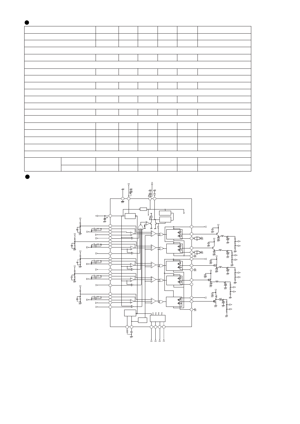
Application Circuit
Symbol
Min.
Max.
Unit
Conditions
Typ.
Parameter
Triangular oscillator)
fosc1
0.179
Vcc-0.4
-
-
2.0
-0.3
0.200
Vcc-0.2
0.2
-
-
-
-
0.221
-
-
0.4
-30
-
0.3
MHz
V
V
mA
mA
V
V
VSATH
VSATL
I
OSOURCE
Iosink
VSTBH
VSTBL
Oscillating frequency
(Output)
Output voltage "H" at operating
Output voltage "L" at operating
Maximum output source current
Maximum output sink current
(STB1
~
5)
STB pin
control voltage
Operating
Non-operating
RT=24k
Ω, CT=220pF
Io=10mA
Io=-10mA
SCP pin detection voltage
NON5
FB5
INV5
FB4
INV4
INV3
FB3
FB2
INV2
Pch DRIVER
Pch DRIVER
Pch DRIVER
Pch DRIVER
Nch DRIVER
REG A
VOLTAGE
REFERENCE
U.V.L.O
TRIANGLE
OSC
FORM
OSC
BUFFER
ON/OFF
LOGIC
PV
CC
1
OUT1
RBIAS1
OUT2
RBIAS2
PGND1
PVCC2
OUT3
RBIAS3
OUT4
RBIAS4
RBIAS5
OUT5
PGND2
SCP5
STB5
STB1
CT
RT
STB23
STB4
DTC5
SCP4
DTC4
SCP3
DTC3
DTC2
SCP1
NON1
INV1
FB1
DTC1
VREF
To Control
To-Divers
ERRAMP1
ERRAMP2
ERRAMP3
ERRAMP4
ERRAMP5
PWM
COMP.5
PWM
COMP.4
PWM
COMP.3
PWM
COMP.2
PWM
COMP.1
SCP2
Block
SCPcomp1
SCPcomp2
SCPcomp3
SCPcomp4
SCPcomp5
4.7
µF
10
µF
V
CC
VREF
VREF
VREF
VREGA
SCP1
SCP2
SCP3
SCP4
SCP5
VREGA
VREGA
VREGA
VREGA
VREGA
INV1
INV2
INV3
INV5
INV4
SCP5
INV5
V
CC
V
CC
V
CC
SCP4
INV4
V
CC
SCP3
INV3
V
CC
V
CC
SCP2
INV2
V
CC
SCP1
INV1
VCC
GND
VREGA
SCP
V
CC
30
32
33
29
3
2
1
4
5
44
8
7
6
9
10
13
12
11
45
47
48
28
27
15
18
17
16
14
20
22
21
19
25
23
24
26
37
35
36
38
39
42
41
40
43
34
46
TIMER LATCH
S
Q
R
BD9730KV