Examples of accessories – Rainbow Electronics DS1972 User Manual
Page 3
DS1972: 1024-Bit EEPROM iButton
3 of 23
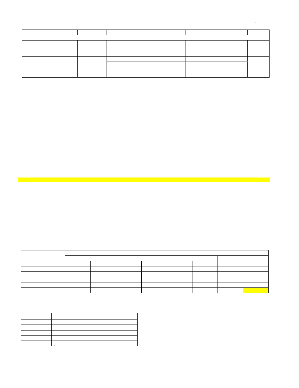
PARAMETER SYMBOL
CONDITIONS
MIN
TYP
MAX
UNITS
EEPROM
Programming Current
I
PROG
(Note 5, 19)
0.8
mA
Programming Time
t
PROG
(Note 20)
10
ms
At 25°C
200k
Write/Erase Cycles (En-
durance) (Notes 21, 22)
N
CY
At 85°C (worst case)
50k
---
Data Retention
(Notes 23, 24)
t
DR
At 85°C (worst case)
10
years
Note 1:
Specifications at T
A
= -40°C are guaranteed by design only and not production-tested.
Note 2:
System requirement.
Note 3:
Maximum allowable pullup resistance is a function of the number of 1-Wire devices in the system and 1-Wire recovery times. The
specified value here applies to systems with only one device and with the minimum 1-Wire recovery times. For more heavily
loaded systems, an active pullup such as that found in the DS2482-x00, DS2480B, or DS2490 may be required.
Note 4:
Maximum value represents the internal parasite capacitance when V
PUP
is first applied. If a 2.2k
W resistor is used to pull up the
data line, 2.5µs after V
PUP
has been applied the parasite capacitance will not affect normal communications.
Note 5:
Guaranteed by design, characterization and/or simulation only. Not production tested.
Note 6:
V
TL
, V
TH
, and V
HY
are a function of the internal supply voltage which is itself a function of V
PUP
, R
PUP
, 1-Wire timing, and
capacitive loading on IO. Lower V
PUP
, higher R
PUP
, shorter t
REC
, and heavier capacitive loading all lead to lower values of V
TL
, V
TH
,
and V
HY
.
Note 7:
Voltage below which, during a falling edge on IO, a logic 0 is detected.
Note 8:
The voltage on IO needs to be less or equal to V
IL(MAX)
at all times the master is driving IO to a logic-0 level.
Note 9:
Voltage above which, during a rising edge on IO, a logic 1 is detected.
Note 10:
After V
TH
is crossed during a rising edge on IO, the voltage on IO has to drop by at least V
HY
to be detected as logic '0'.
Note 11:
The I-V characteristic is linear for voltages less than 1V.
Note 12:
Applies to a single device attached to a 1-Wire line.
Note 13:
The earliest recognition of a negative edge is possible at t
REH
after V
TH
has been reached on the preceding rising edge.
Note 14:
Defines maximum possible bit rate. Equal to t
W0L(min)
+ t
REC(min)
.
Note 15:
Interval after t
RSTL
during which a bus master is guaranteed to sample a logic-0 on IO if there is a DS1972 present. Minimum limit
is t
PDH(max)
; maximum limit is t
PDH(min)
+ t
PDL(min)
.
Note 16:
Highlighted numbers are NOT in compliance with legacy 1-Wire product standards. See comparison table below.
Note 17:
e represents the time required for the pullup circuitry to pull the voltage on IO up from V
IL
to V
TH
.
Note 18:
d represents the time required for the pullup circuitry to pull the voltage on IO up from V
IL
to the input high threshold of the bus
master.
Note 19:
Current drawn from IO during the EEPROM programming interval. The pullup circuit on IO during the programming interval
should be such that the voltage at IO is greater than or equal to Vpup(min). If Vpup in the system is close to Vpup(min) then a low
impedance bypass of Rpup which can be activated during programming may need to be added.
Note 20:
Interval begins t
WiLMIN
after the leading negative edge on IO for the last timeslot of the E/S byte for a valid Copy Scratchpad
sequence. Interval ends once the device's self-timed EEPROM programming cycle is complete and the current drawn by the
device has returned from I
PROG
to I
L
.
Note 21:
Write-cycle endurance is degraded as T
A
increases.
Note 22:
Not 100% production-tested; guaranteed by reliability monitor sampling.
Note 23:
Data retention is degraded as T
A
increases.
Note 24:
Guaranteed by 100% production test at elevated temperature for a shorter time; equivalence of this production test to data sheet
limit at operating temperature range is established by reliability testing.
LEGACY VALUES
DS1972 VALUES
PARAMETER
STANDARD SPEED
OVERDRIVE SPEED
STANDARD SPEED
OVERDRIVE SPEED
MIN MAX MIN MAX MIN MAX MIN MAX
t
SLOT
(incl. t
REC
)
61µs (undef.) 7µs (undef.) 65µs
1)
(undef.) 8µs
1)
(undef.)
t
RSTL
480µs
(undef.) 48µs 80µs 480µs 640µs 48µs 80µs
t
PDH
15µs 60µs 2µs 6µs 15µs 60µs 2µs 6µs
t
PDL
60µs 240µs 8µs 24µs 60µs 240µs 8µs 24µs
t
W0L
60µs 120µs 6µs 16µs 60µs 120µs 6µs 15.5µs
1)
Intentional change, longer recovery time requirement due to modified 1-Wire front end.
EXAMPLES OF ACCESSORIES
PART DESCRIPTION
DS9096P
Self-Stick Adhesive Pad
DS9101 Multipurpose
Clip
DS9093RA
Mounting Lock Ring
DS9093A Snap-In
Fob
DS9092 iButton Probe