Dc and logic electrical characteristics, Converter electrical characteristics – Rainbow Electronics ADC12010 User Manual
Page 6
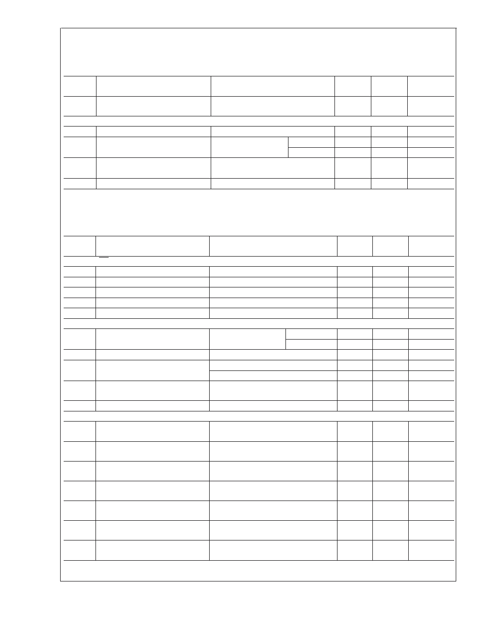
Converter Electrical Characteristics
(Continued)
Unless otherwise specified, the following specifications apply for AGND = DGND = DR GND = 0V, V
A
= V
D
= +5V, V
DR
=
+3.0V, PD = 0V, V
REF
= +2.0V, f
CLK
= 10 MHz, t
r
= t
f
= 3 ns, C
L
= 25 pF/pin. Boldface limits apply for T
A
= T
J
= T
MIN
to
T
MAX
: all other limits T
A
= T
J
= 25˚C (Notes 7, 8, 9)
Symbol
Parameter
Conditions
Typical
Limits
Units
(Limits)
IMD
Intermodulation Distortion
f
IN
= 4.7 MHz and 4.9 MHz,
each = −7 dBFS
−75
dBFS
REFERENCE AND ANALOG INPUT CHARACTERISTICS
V
CM
Common Mode Input Voltage
V
A
/ 2
V
C
IN
V
IN
Input Capacitance (each pin to
GND)
V
IN
= 2.5 Vdc
+ 0.7 V
rms
(CLK LOW)
8
pF
(CLK HIGH)
7
pF
V
REF
Reference Voltage (Note 13)
2.00
1.0
V (min)
2.4
V (max)
Reference Input Resistance
100
M
Ω(min)
DC and Logic Electrical Characteristics
Unless otherwise specified, the following specifications apply for AGND = DGND = DR GND = 0V, V
A
= V
D
= +5V, V
DR
=
+3.0V, PD = 0V, V
REF
= +2.0V, f
CLK
= 10 MHz, t
r
= t
f
= 3 ns, C
L
= 25 pF/pin. Boldface limits apply for T
A
= T
J
= T
MIN
to
T
MAX
: all other limits T
A
= T
J
= 25˚C (Notes 7, 8, 9)
Symbol
Parameter
Conditions
Typical
Limits
Units
(Limits)
CLK, PD, OE DIGITAL INPUT CHARACTERISTICS
V
IN(1)
Logical “1” Input Voltage
V
D
= 5.25V
2.0
V (min)
V
IN(0)
Logical “0” Input Voltage
V
D
= 4.75V
1.0
V (max)
I
IN(1)
Logical “1” Input Current
V
IN
= 5.0V
10
µA
I
IN(0)
Logical “0” Input Current
V
IN
= 0V
−10
µA
C
IN
Digital Input Capacitance
5
pF
D0–D11 DIGITAL OUTPUT CHARACTERISTICS
V
OUT(1)
Logical “1” Output Voltage
I
OUT
= −0.5 mA
V
DR
= 2.5V
2.3
V (min)
V
DR
= 3V
2.7
V (min)
V
OUT(0)
Logical “0” Output Voltage
I
OUT
= 1.6 mA, V
DR
= 3V
0.4
V (max)
I
OZ
TRI-STATE Output Current
V
OUT
= 2.5V or 5V
100
nA
V
OUT
= 0V
−100
nA
+I
SC
Output Short Circuit Source
Current
V
OUT
= 0V
−20
mA (min)
−I
SC
Output Short Circuit Sink Current
V
OUT
= V
DR
20
mA (min)
POWER SUPPLY CHARACTERISTICS
I
A
Analog Supply Current
PD Pin = DGND, V
REF
= 2.0V
PD Pin = V
DR
30
2.8
39
mA (max)
mA
I
D
Digital Supply Current
PD Pin = DGND
PD Pin = V
DR
, f
CLK
= 0
2
2.2
2.5
mA (max)
mA
I
DR
Digital Output Supply Current
PD Pin = DGND, C
L
= 0 pF (Note 14)
PD Pin = V
DR
, f
CLK
= 0
0
0
mA
mA
Total Power Consumption
PD Pin = DGND, C
L
= 0 pF (Note 15)
PD Pin = V
DR
, f
CLK
= 0
160
25
207
mW
mW
PSRR1+
Power Supply Rejection Ratio
Rejection of Positive Full-Scale Error
with V
A
= 4.75V vs. 5.25V
69
dBFS
PSRR1−
Power Supply Rejection Ratio
Rejection of Negative Full-Scale Error
with V
A
= 4.75V vs. 5.25V
51
dBFS
PSRR2
Power Supply Rejection Ratio
Rejection of Power Supply Noise with
10 MHz, 250 mV
P-P
riding on V
A
48
dBFS
ADC12010
www.national.com
6