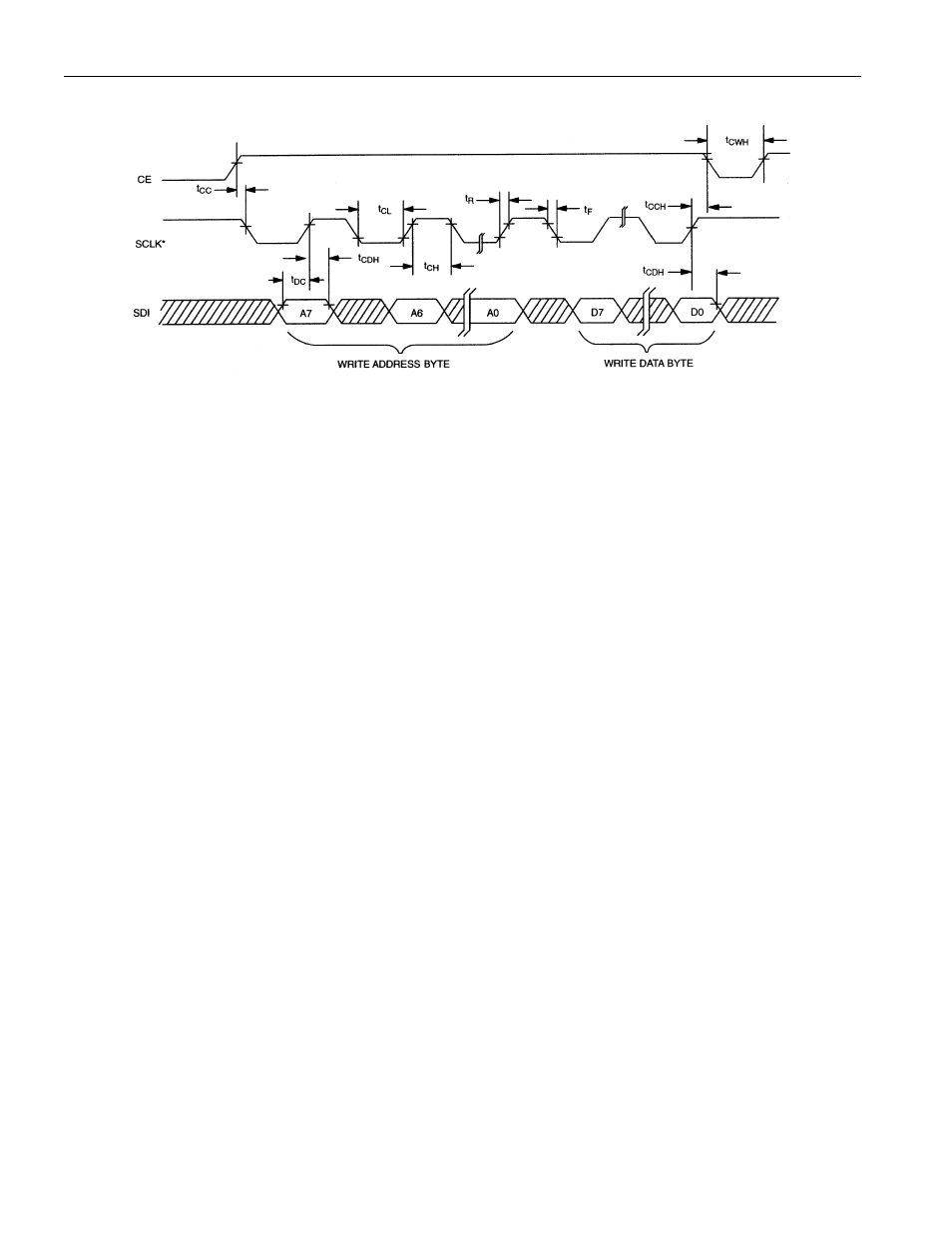
Timing diagram: spi write data transfer figure 12 – Rainbow Electronics DS1722 User Manual
Page 12

DS1722
12 of 13
TIMING DIAGRAM: SPI WRITE DATA TRANSFER Figure 12
*SCLK can be either polarity, timing shown for CPOL = 1.
NOTES:
1. All voltages are referenced to ground.
2. Logic 0 voltages are specified at a sink current of 4 mA.
3. Logic 1 voltages are specified at a source current of 1 mA.
4. I
CC
specified with SCLK=V
DDD
and CE=GND. Typical I
CC1
is 0.25 µA and I
CC
is 0.3 mA at 25°C
and V
DDD =
2.65V
.
5. Measured at V
IH
=0.7 V
DDD
or V
IL
=0.2 V
DDD
and 10 ms maximum rise and fall time.
6. Measured with 50 pF load
7. Measured at V
OH
=0.7 V
DDD
or V
OL
=0.2 V
DDD
. Measured from the 50% point of SCLK to the V
OH
minimum of SDO.
8. Figure 13 shows mean thermometer error for a pre-characterization sample. Data covering a larger
sample over the full temperature range is pending.
- MAX5151 (16 pages)
- MAXQ3108 (64 pages)
- MAX5661 (39 pages)
- MAX6691 (7 pages)
- MAX5362 (12 pages)
- ADC10158 (26 pages)
- MAX8922L (14 pages)
- MAX8596Z (8 pages)
- MAX7491 (18 pages)
- MAX15040 (15 pages)
- MAX5177 (16 pages)
- ADC08138 (22 pages)
- MAX5961 (42 pages)
- T89C51RD2 (86 pages)
- MAX16055 (9 pages)
- MAX6659 (17 pages)
- ADC0820 (20 pages)
- MAX6678 (19 pages)
- MAX8884Z (15 pages)
- MAX16915 (9 pages)
- MAX8620 (18 pages)
- MAX5144 (12 pages)
- MAX6670 (8 pages)
- MAX8760 (39 pages)
- W78C32C (14 pages)
- MX7533 (8 pages)
- MAX8727 (13 pages)
- MAX9053 (15 pages)
- W78C54 (16 pages)
- MAX8614B (15 pages)
- W90N740 (219 pages)
- MAX6626 (13 pages)
- ADC10738 (30 pages)
- MAX17000 (31 pages)
- MAX5051 (21 pages)
- MAXQ1004 (18 pages)
- MAX6871 (51 pages)
- MX7847 (12 pages)
- MAX6608 (6 pages)
- MAX17083 (15 pages)
- MAX6641 (17 pages)
- MAX5251 (16 pages)
- MAX6338 (8 pages)
- MAX6690 (16 pages)
- MAX8668 (18 pages)
