Rainbow Electronics ADC12020 User Manual
General description, Features, Key specifications

ADC12020
12-Bit, 20 MSPS, 185 mW A/D Converter with Internal
Sample-and-Hold
General Description
The ADC12020 is a monolithic CMOS analog-to-digital con-
verter capable of converting analog input signals into 12-bit
digital words at 20 Megasamples per second (MSPS), mini-
mum. This converter uses a differential, pipeline architecture
with digital error correction and an on-chip sample-and-hold
circuit to minimize die size and power consumption while
providing excellent dynamic performance. Operating on a
single 5V power supply, this device consumes just 185 mW
at 20 MSPS, including the reference current. The Power
Down feature reduces power consumption to 40 mW.
The differential inputs provide a full scale input swing equal
to 2V
REF
with the possibility of a single-ended input. Full use
of the differential input is recommended for optimum perfor-
mance. For ease of use, the buffered, high impedance,
single-ended reference input is converted on-chip to a differ-
ential reference for use by the processing circuitry. Output
data format is 12-bit offset binary.
This device is available in the 32-lead LQFP package and
will operate over the industrial temperature range of −40˚C to
+85˚C.
Features
n
Internal sample-and-hold
n
Outputs 2.5V to 5V compatible
n
TTL/CMOS compatible input/outputs
n
Power down mode
n
On-chip reference buffer
Key Specifications
n
Resolution
12 Bits
n
Conversion Rate
20 MSPS (min)
n
DNL
±
0.35 LSB (typ)
n
INL
±
0.55 LSB (typ)
n
SNR (f
IN
= 10.1 MHz)
70 dB (typ)
n
ENOB (f
IN
= 10.1 MHz)
11.3 bits (typ)
n
Data Latency
6 Clock Cycles
n
Supply Voltage
+5V
±
5%
n
Power Consumption, 20 MHz
185 mW (typ)
Applications
n
Image Processing Front End
n
Instrumentation
n
PC-Based Data Acquisition
n
Fax Machines
n
Waveform Digitizers
n
Sonar/Radar
n
DSP Front Ends
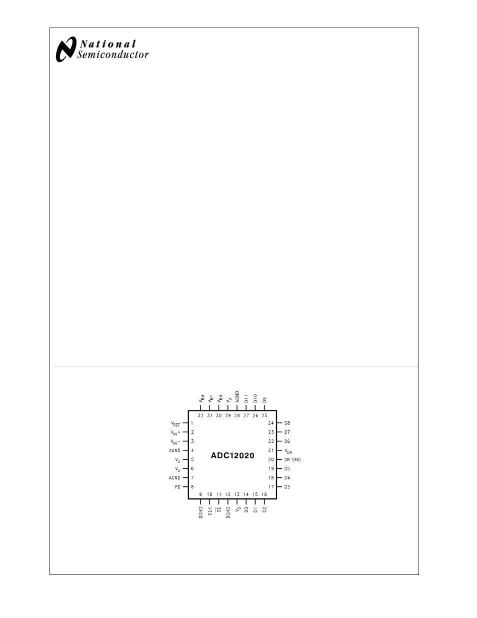
Connection Diagram
20051701
TRI-STATE
®
is a registered trademark of National Semiconductor Corporation.
April 2003
ADC12020
12-Bit,
20
MSPS,
185
mW
A/D
Converter
with
Internal
Sample-and-Hold
© 2003 National Semiconductor Corporation
DS200517
www.national.com
Document Outline
- ADC12020
- General Description
- Features
- Key Specifications
- Applications
- Connection Diagram
- Ordering Information
- Block Diagram
- Pin Descriptions and Equivalent Circuits
- Absolute Maximum Ratings
- Operating Ratings (Notes , )
- Converter Electrical Characteristics
- DC and Logic Electrical Characteristics
- AC Electrical Characteristics
- Specification Definitions
- Timing Diagram
- Transfer Characteristic
- ADC12020 Typical Performance Characteristics
- Functional Description
- Applications Information
- 1.0 OPERATING CONDITIONS
- 1.1 Analog Inputs
- 1.2 Reference Pins
- 1.3 Signal Inputs
- FIGURE 2. Expected Input Signal Range
- FIGURE 3. Angular Errors Between the Two Input Signals Will Reduce the Output Level
- TABLE 1. Input to Output Relationship- Differential Input
- TABLE 2. Input to Output Relationship- Single-Ended Input
- 1.3.1 Single-Ended Operation
- 1.3.2 Driving the Analog Inputs
- 1.3.3 Input Common Mode Voltage
- 2.0 DIGITAL INPUTS
- 3.0 OUTPUTS
- 4.0 POWER SUPPLY CONSIDERATIONS
- 5.0 LAYOUT AND GROUNDING
- 6.0 DYNAMIC PERFORMANCE
- 7.0 COMMON APPLICATION PITFALLS
- 1.0 OPERATING CONDITIONS
- Physical Dimensions
