Overview, 1 block diagram, Atmega1284p – Rainbow Electronics ATmega1284P User Manual
Page 3

3
8059CS–AVR–07/09
ATmega1284P
2.
Overview
The ATmega1284P is a low-power CMOS 8-bit microcontroller based on the AVR enhanced
RISC architecture. By executing powerful instructions in a single clock cycle, the ATmega1284P
achieves throughputs approaching 1 MIPS per MHz allowing the system designer to optimize
power consumption versus processing speed.
2.1
Block Diagram
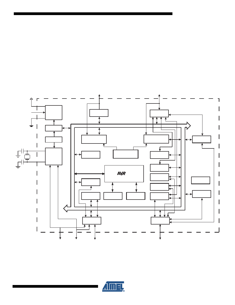
Figure 2-1.
Block Diagram
The AVR core combines a rich instruction set with 32 general purpose working registers. All the
32 registers are directly connected to the Arithmetic Logic Unit (ALU), allowing two independent
registers to be accessed in one single instruction executed in one clock cycle. The resulting
architecture is more code efficient while achieving throughputs up to ten times faster than con-
ventional CISC microcontrollers.
CPU
GND
VCC
RESET
Power
Supervision
POR / BOD &
RESET
Watchdog
Oscillator
Watchdog
Timer
Oscillator
Circuits /
Clock
Generation
XTAL1
XTAL2
PORT A (8)
PORT D (8)
PD7..0
PORT C (8)
PC5..0
TWI
SPI
EEPROM
JTAG/OCD
16bit T/C 1
8bit T/C 2
8bit T/C 0
SRAM
FLASH
USART 0
Internal
Bandgap reference
Analog
Comparator
A/D
Converter
PA7..0
PORT B (8)
PB7..0
USART 1
TOSC1/PC6
TOSC2/PC7
16bit T/C 1
16bit T/C 3
