Rainbow Electronics BD6111FV User Manual
Bd6111fv
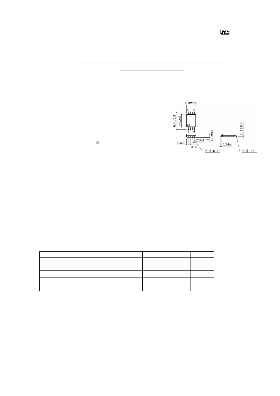
Dimension
(Units:mm)
Description
Applications
Features
Variable output, negative voltage IC
BD6111FV
99W028A
Maximum applied power supply voltage
Power dissipation
Operating temperature range
Storage temperature
V
BAT
Pd
Topr
Tstg
V
IN
V
˚C
˚C
Unit
V
mW
300
-20
+70
-55
+125
Symbol
Limits
-0.3
+6.0
-0.3
+6.0
Parameter
Maximum applied input voltage
~
~
~
~
Absolute Maximum Ratings (Ta=25
˚C
)
*
December, 1999
The BD6111FV is a charge-pump, negative supply IC
containing a regulator. The charge pump block inverts
a positive power supply voltage that is inputted to
VBAT pin into a negative voltage and outputs it from
the NEGOUT pin. The regulator block stabilizes this
negative voltage with low-noise and outputs it from
OUT pin. Output voltage values of this regulator can
be controlled by voltage value inputted to VIN pin and
determined by OUT=-1.6 VIN .
1) Highly efficient, built-in inverting charge pump
2) Built-in variable, negative voltage linear regulator.
3) Built-in stand-by switch circuit (pull down resistor 1M
Ω)
4) Compact SSOP-B8 package
SSOP-B8
Compact information computer terminal, such as PDC, PHS and PDA.
Battery driving apparatus requiring negative voltage.
*Derating:3.0mW/˚C for operation above Ta=25˚C.