Applications information, Pin description – Rainbow Electronics MAX6160 User Manual
Page 7

_______________________________________________________________________________________
7
_____________Applications Information
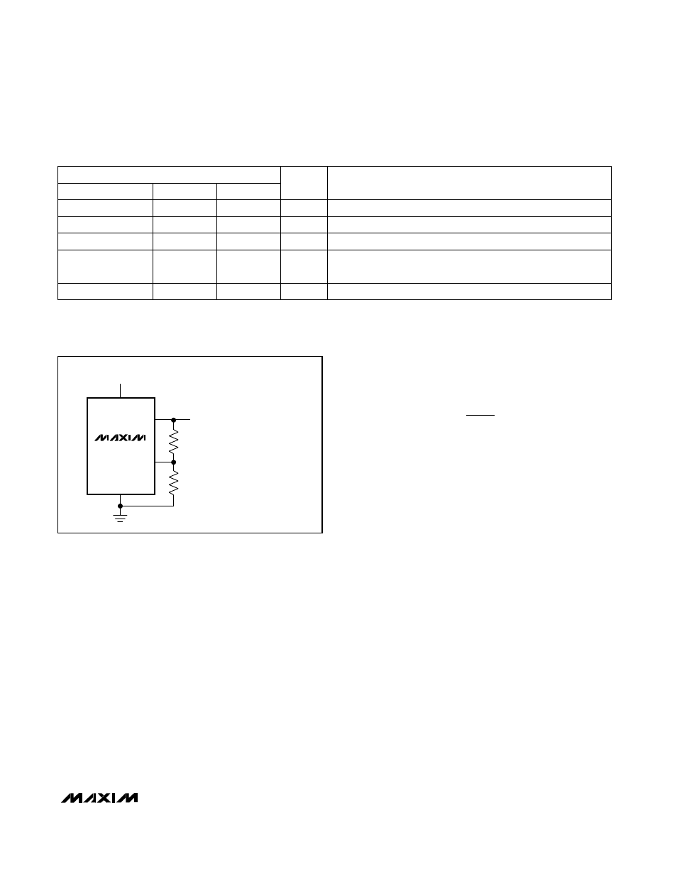
Setting the MAX6160 Output Voltage
Set the output voltage on the MAX6160 by connecting
a resistor divider between OUT, ADJ, and GND
(Figure 1). Choose R1 according to the following equa-
tion:
R1 = (1.06 x 10
5
) (V
OUT
/ V
ADJ
)(k
Ω
)
where V
TH
= 1.23V. The scaling factor (1.06 x 10
5
)
compensates for the MAX6160's change in ADJ input
current over temperature. When R1 is chosen correctly,
the change in voltage across R1 caused by the ADJ
input current is properly cancelled. Choose R1 to within
±5% of this calculated value (nearest standard value
plus specified resistor tolerance) to optimize the output
voltage temperature coefficient. Using R1 = 215k
Ω
:
which is also the nearest 0.1% resistor value.
Choose R2 according to the following equation:
R2 = R1 / (V
OUT
/ V
ADJ
- 1)
For example, a 2.5V output requires R1 = (1.06 x 10
5
)
(2.5V / 1.23V)
≈
215
Ω
, which is the nearest standard-
value 0.1% resistor.
Input Bypassing
For the best line-transient performance, decouple the
input with a 0.1µF ceramic capacitor, as shown in the
Typical Operating Circuit
. Locate the capacitor as
close to the device pin as possible. Where transient
performance is less important, no capacitor is
necessary.
Output Bypassing
The MAX6125/MAX6141/MAX6145/MAX6150/MAX6160
do not require an output capacitor. They are stable for
capacitive loads from 0nF to 10nF. If your application
requires an output charge reservoir (e.g., to decouple
the reference from a DAC’s input), then make sure that
the total output capacitive load does not exceed 10nF
for optimum settling-time performance.
MAX6125/MAX6141/MAX6145/MAX6150/MAX6160
SOT23, Low-Cost, Low-Dropout,
3-Terminal Voltage References
______________________________________________________________Pin Description
Adjustable output voltage feedback input. Connect a resistor
divider between OUT, ADJ, and GND (Figure 1).
ADJ
5**
Input Voltage
IN
8
Ground
GND
4
No Connection. Not internally connected.
N.C.
2, 3, 5*, 6, 7
Reference Output
OUT
1
FUNCTION
NAME
SO
—
1
3
—
2
SOT23-3
2
3
1
—
4
SOT143
*
Except MAX6160.
**
MAX6160 only.
MAX6160
OUT
ADJ
GND
IN
R1 = 1.06 x 10
5
(
––––
)
( k
Ω
)
V
OUT
V
ADJ
R2 = –—––––
V
OUT
V
ADJ
(
–––– - 1
)
R1
V
ADJ
= 1.23V
V
OUT
V
IN
R1
R2
Figure 1. MAX6160 Adjustable Output Circuit
PIN
R2 = 215k
2.5V
1.23V
- 1
208k
Ω
≈
Ω
,
