Applications information – Rainbow Electronics MAX5971А User Manual
Page 19

______________________________________________________________________________________ 19
MAX5971A
Single-Port, 40W, IEEE 802.3af/802.3at PSE
Controller with Integrated MOSFET
The MAX5971A also contains an internal square wave,
PWM signal generator. The PWM runs at a typical fre-
quency of 25kHz with an approximate typical duty cycle
of 6.25%. PWMEN is used to enable or disable the PWM.
PWMEN is internally pulled up to the digital supply, and
can be left unconnected to enable the internal PWM.
When enabled, the LED pulses are driven by the PWM
to reduce the power dissipation and increase the system
efficiency. Force PWMEN low to disable the internal
PWM; the LED is then driven directly.
Thermal Shutdown
If the MAX5971A die temperature reaches 150NC, an
overtemperature fault is generated and the device shuts
down. The die temperature must cool down below 130NC
to remove the overtemperature fault condition. After a
thermal shutdown condition clears, the device is reset.
Applications Information
Layout Procedure
Careful PCB layout is critical to achieve high efficiency
and low EMI. Follow these layout guidelines for optimal
performance.
1) Place the input bypass capacitance and the output
bypass capacitor (0.1µF ceramic capacitor from
AGND to OUTP) as close to the MAX5971A as pos-
sible.
2) Use large SMT component pads for power dissipat-
ing devices such as the MAX5971A and the external
diodes in the high-power path.
3) Use short, wide traces whenever possible for high-
power paths.
4) Use the MAX5971 Evaluation Kit as a design and
layout reference.
5) The exposed pad (EP) must be soldered evenly to the
PCB ground plane for proper operation and power
dissipation. Use multiple vias beneath the exposed
paddle for maximum heat dissipation. A 1.0mm to
1.2mm pitch is the recommended spacing for these
vias and they should be plated (1oz copper) with a
small barrel diameter (0.30mm to 0.33mm).
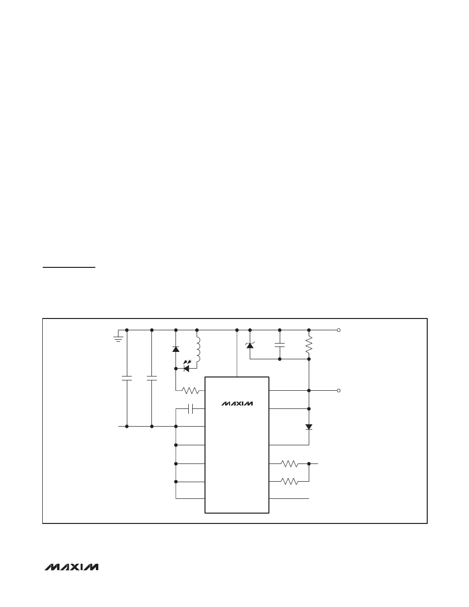
Figure 6. Typical Operating Circuit 1 (DC Load Removal Detection, Internal PWM Enabled for LED Indication, and Class 5
Detection Enabled)
1N4448
1kI
1kI
1nF
-54V
5.1kI
LED
10mH
1N4448
0.1µF
100V
47µF
100V
-54V
LED
AGND
EN
V
EE
V
EE_DIG
LEGACY
MIDSPAN
OSC
OUT
OUTP
DET
ILIM1
ILIM2
PWMEN
MAX5971A
0.1µF
100V
SMJ58A
2.2MI
PSE OUTPUT
