Detailed description – Rainbow Electronics MAX5264 User Manual
Page 9
MAX5264
Octal, 14-Bit Voltage-Output DAC
with Parallel Interface for ATE
_______________________________________________________________________________________
9
_______________Detailed Description
Analog Section
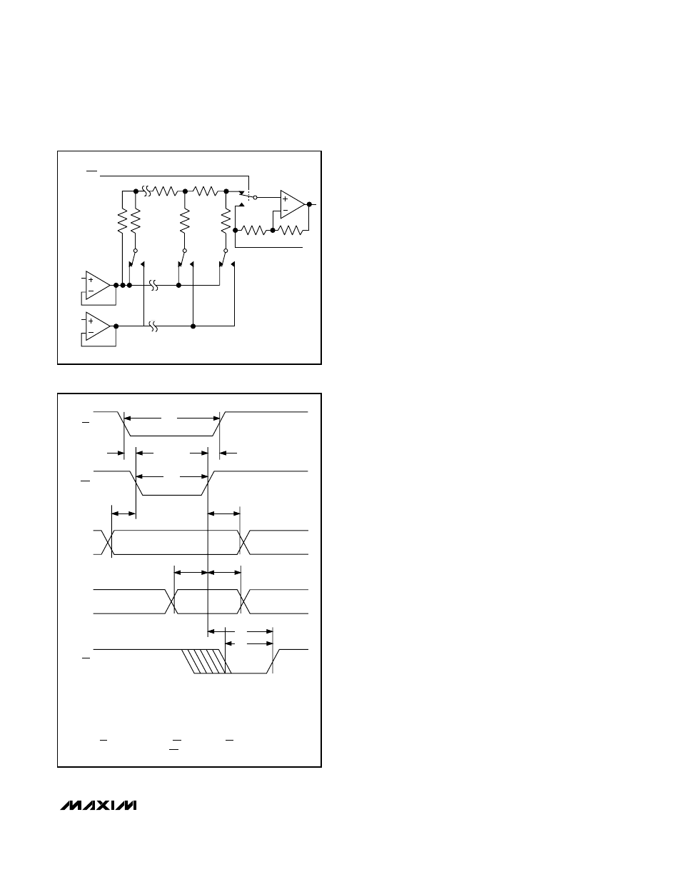
The MAX5264 contains eight 14-bit voltage-output
DACs. These DACs are “inverted” R-2R ladder net-
works that convert 14-bit digital inputs into equivalent
analog output voltages, in proportion to the applied ref-
erence voltages (Figure 1). The MAX5264 has three
positive reference inputs (REF_ _ _ _+) and three nega-
tive reference inputs (REF_ _ _ _-). The difference from
REF_ _ _ _+ to REF_ _ _ _-, multiplied by two, sets the
DAC output span.
In addition to the differential reference inputs, the
MAX5264 has four analog-ground input pins (DUT-
GND_ _). When CLR is high (unasserted), the voltage
on DUTGND_ _ offsets the DAC output voltage range. If
CLR is asserted, the output amplifier is forced to the
voltage present on DUTGND_ _.
Reference and DUTGND Inputs
All of the MAX5264’s reference inputs are buffered with
precision amplifiers. This allows the flexibility of using
resistive dividers to set the reference voltages. Because
of the relatively high multiplying bandwidth of the refer-
ence input (188kHz), any signal present on the refer-
ence pin within this bandwidth is replicated on the DAC
output.
The DUTGND pins of the MAX5264 are connected to
the negative source resistor (nominally 115k
Ω) of the
output amplifier. The DUTGND pins are typically con-
nected directly to analog ground. Each of these pins
has an input current that varies with the DAC digital
code. If the DUTGND pins are driven by external cir-
cuitry, budget ±200µA per DAC for load current.
Output Buffer Amplifiers
The MAX5264’s voltage outputs are internally buffered
by precision gain-of-two amplifiers with a typical slew
rate of 1V/µs. With a full-scale transition at its output,
the typical settling time to ±1LSB is 22µs. This settling
time does not significantly vary with capacitive loads
less than 10,000pF.
Output Deglitching Circuit
The MAX5264’s internal connection from the DAC lad-
der to the output amplifier contains special deglitch cir-
cuitry. This glitch/deglitch circuitry is enabled on the
falling edge of LD to remove the glitch from the R-2R
DAC. This enables the MAX5264 to exhibit a fraction of
the glitch impulse energy of parts without the deglitch-
ing circuit.
REF-
REF+
2R
2R
2R
2R
2R
OUT
DUTGND
2R
CLR
R
R
D0
D12
D13
Figure 1. DAC Simplified Circuit
CS
WR
A0–A2
D0–D13
LD
NOTES:
(NOTE 3)
1. ALL INPUT RISE AND FALL TIMES MEASURED FROM 10% TO 90% OF
+5V. t
r
= t
f
= 5ns.
2.
3.
t
1
t
2
t
8
t
9
t
6
t
7
t
4
t
5
t
3
t
3
MEASUREMENT REFERENCE LEVEL IS (V
INH
+ V
INL
) / 2.
IF LD IS ACTIVATED WHILE WR IS LOW, THEN LD MUST STAY LOW
FOR t
3
OR LONGER AFTER WR GOES HIGH.
Figure 2. Digital Timing Diagram