Functional description, Applications information – Rainbow Electronics ADC16061 User Manual
Page 13
Functional Description
Operating on a single +5V supply, the ADC16061 uses a
pipelined architecture and has error correction circuitry and a
calibration mode to help ensure maximum performance at all
times.
Balanced analog signals with a peak-to-peak voltage equal
to the input reference voltage, V
REF
, and centered around
the common mode input voltage, V
CM
, are digitized to 16 bits
(15 bits plus sign). Neglecting offsets, positive input signal
voltages (V
IN
+ − V
IN
−
≥
0) produce positive digital output
data and negative input signal voltages (V
IN
+ − V
IN
−
<
0)
produce negative output data. The input signal can be digi-
tized at any clock rate between 300 Ksps and 2.5 Msps.
Input voltages below the negative full scale value will cause
the output word to take on the negative full scale value of
1000,0000,0000,0000. Input voltage above the positive full
scale value will cause the output word to take on the positive
full scale value of 0111,1111,1111,1111.
The output word rate is the same as the clock frequency. The
analog input voltage is acquired at the falling edge of the
clock and the digital data for that sample is delayed by the
pipeline for 13 clock cycles plus t
DATA_VALID
. The digital out-
put is undefined if the chip is being reset or is in the calibra-
tion mode. The output signal may be inhibited by the RD pin
while the converter is in one of these modes.
Applications Information
1.0 OPERATING CONDITIONS
We recommend that the following conditions be observed for
operation of the ADC16061:
4.75V
≤
V
A
≤
5.25V
5.25V
≤
V
D
≤
5.25V
3.0V
≤
V
D
I/O
≤
V
D
0.3MHz
≤
f
CLK
≤
2.5 MHz
V
CM
= 2.0V (forced)
V
REF IN
+ = 2.0V
V
REF IN
− = AGND
1.1 The Analog Inputs
The ADC16061 has two analog signal inputs, V
IN
+ and V
IN
−.
These two pins form a balanced input. There are two refer-
ence pins, V
REF
+
IN
and V
REF
−
IN
. These pins form a differ-
ential input reference.
1.2 Reference Inputs
V
REF
+
IN
should always be more positive than V
REF
−
IN
. The
effective reference voltage, V
REF
, is the difference between
these two voltages:
V
REF
= (V
REF
+
IN
) − (V
REF
−
IN
).
The operational voltage range of V
REF
+
IN
is +1.8 Volts to
+3.0 Volts. The operational voltage range of V
REF
−
IN
is
ground to 1.0V. For best performance, the difference be-
tween V
REF
+
IN
and V
REF
−
IN
should remain within the range
of 1.8V to 2.2V. Reducing the reference voltage below 1.8V
will decrease the signal-to-noise ratio (SNR) of the
ADC16061. Increasing the reference voltage (and, conse-
quently, the input signal swing) above 2.2V will increase
THD.
V
REF (MID)
is the reference mid-point and is derived from
V
CM
. This point is brought out only to be by passed. Bypass
this pin with 0.1µF capacitor to ground. Do not load this pin.
It is very important that all grounds associated with the refer-
ence voltage make connection to the analog ground plane at
a single point to minimize the effects of noise currents in the
ground path.
1.3 Signal Inputs
The signal inputs are V
IN
+ and V
IN
−. The signal input, V
IN
,
is defined as
V
IN
= (V
IN
+) − (V
IN
−).
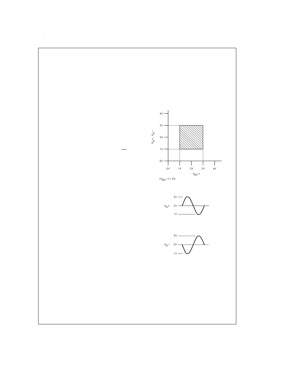
Figure 3
indicates the relationship between the input voltage
and the reference voltages.
Figure 4
shows the expected in-
put signal range.
The ADC16061 performs best with a balanced input cen-
tered around V
CM
. The peak-to-peak voltage swing at either
V
IN
+ or V
IN
− should be less than the reference voltage and
each signal input pin should be centered on the V
CM
voltage.
The two V
CM
-centered input signals should be exactly 180˚
out of phase from each other. As a simple check to ensure
this, be certain that the average voltage at the ADC input
pins is equal to V
CM
. Drive the analog inputs with a source
impedance less than 100 Ohms.
The sign bit of the output word will be a logic low when V
IN
+
is greater than V
IN
− . When V
IN
+ is less than V
IN
−, the sign
bit of the output word will be a logic high.
DS100889-17
FIGURE 3. Typical Input to Reference Relationship.
DS100889-18
FIGURE 4. Expected Input Signal Range.
www.national.com
13