Electrical characteristics (continued) – Rainbow Electronics MAX5302 User Manual
Page 3
MAX5302
Low-Power, 12-Bit Voltage-Output DAC
with Serial Interface
_______________________________________________________________________________________
3
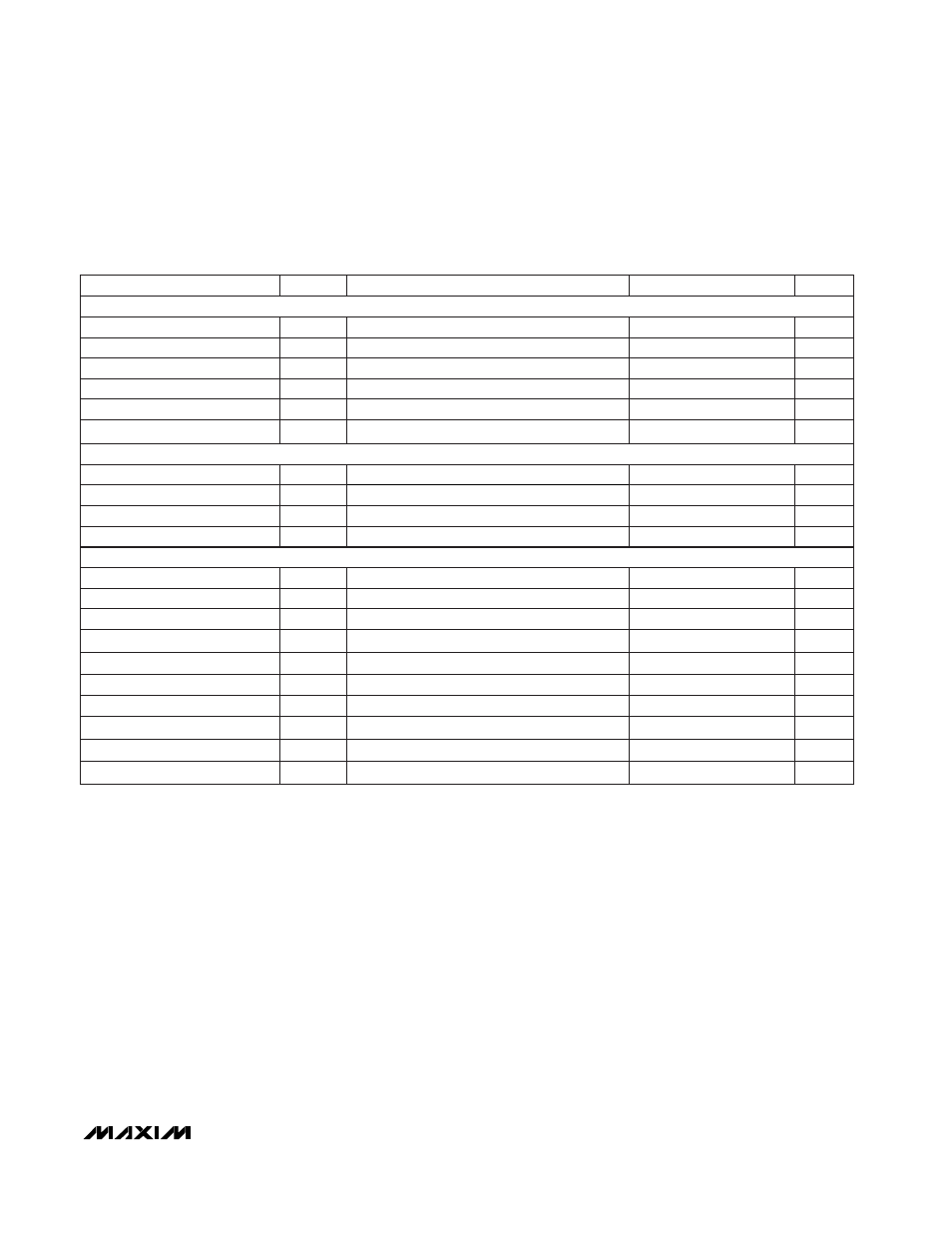
(Note 3)
CS = V
DD
, DIN = 100kHz
Rail-to-rail (Note 2)
To ±1/2LSB, V
STEP
= 2.5V
CONDITIONS
mA
0.28
0.4
I
DD
Supply Current
V
4.5
5.5
V
DD
Supply Voltage
nVs
5
Digital Feedthrough
µs
20
Start-Up Time
µA
0.001
±0.1
Current into FB
V
0 to V
DD
Output Voltage Swing
µs
14
Output Settling Time
V/µs
0.6
SR
Voltage Output Slew Rate
UNITS
MIN
TYP
MAX
SYMBOL
PARAMETER
(Note 3)
µA
4
20
Supply Current in Shutdown
µA
0.001
±0.5
Reference Current in Shutdown
ns
40
t
CH
SCLK Pulse Width High
ns
100
t
CP
SCLK Clock Period
ns
40
t
CSS
CS Fall to SCLK Rise Setup Time
ns
40
t
DS
DIN Setup Time
ns
0
t
CSH
SCLK Rise to CS Rise Hold Time
ns
40
t
CL
SCLK Pulse Width Low
ns
40
t
CS1
CS Rise to SCLK Rise Hold Time
ns
100
t
CSW
CS Pulse Width High
ns
40
t
CS0
SCLK Rise to CS Fall Delay
ns
0
t
DH
DIN Hold Time
Note 1: Guaranteed from code 11 to code 4095 in unity-gain configuration.
Note 2: Accuracy is better than 1LSB for V
OUT
= 8mV to (V
DD
- 100mV), guaranteed by a power-supply rejection test at the end
points.
Note 3: R
L
=
∞, digital inputs at GND or V
DD
.
DIGITAL INPUTS
DYNAMIC PERFORMANCE
POWER SUPPLIES
TIMING CHARACTERISTICS (Figure 6)
ELECTRICAL CHARACTERISTICS (continued)
(Circuit of Figure 8, V
DD
= +5V ±10%, V
REF
= +2.5V, R
L
= 5k
Ω, C
L
= 100pF, T
A
= T
MIN
to T
MAX
, unless otherwise noted. Typical val-
ues are at T
A
= +25°C. Output buffer connected in unity-gain configuration.)