Functional description – Rainbow Electronics ADC0838 User Manual
Page 14
Functional Description
(Continued)
4 When the start bit has been shifted into the start location
of the MUX register the input channel has been assigned
and a conversion is about to begin An interval of
clock
period (where nothing happens) is automatically inserted to
allow the selected MUX channel to settle The SAR status
line goes high at this time to signal that a conversion is now
in progress and the DI line is disabled (it no longer accepts
data)
5 The data out (DO) line now comes out of TRI-STATE and
provides a leading zero for this one clock period of MUX
settling time
6 When the conversion begins the output of the SAR com-
parator which indicates whether the analog input is greater
than (high) or less than (low) each successive voltage from
the internal resistor ladder appears at the DO line on each
falling edge of the clock This data is the result of the con-
version being shifted out (with the MSB coming first) and
can be read by the processor immediately
7 After 8 clock periods the conversion is completed The
SAR status line returns low to indicate this
clock cycle
later
8 If the programmer prefers the data can be provided in an
LSB first format this makes use of the shift enable (SE)
control line
All 8 bits of the result are stored in an output
shift register On devices which do not include the SE con-
trol line the data LSB first is automatically shifted out the
DO line after the MSB first data stream The DO line then
goes low and stays low until CS is returned high On the
ADC0838 the SE line is brought out and if held high the
value of the LSB remains valid on the DO line When SE is
forced low the data is then clocked out LSB first The
ADC0831 is an exception in that its data is only output in
MSB first format
9 All internal registers are cleared when the CS line is high
If another conversion is desired CS must make a high to
low transition followed by address information
The DI and DO lines can be tied together and controlled
through a bidirectional processor I O bit with one wire This
is possible because the DI input is only ‘‘looked-at’’ during
the MUX addressing interval while the DO line is still in a
high impedance state
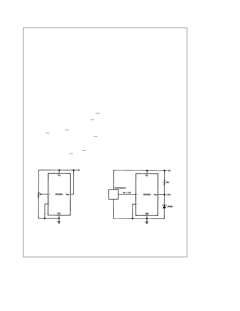
3 0 REFERENCE CONSIDERATIONS
The voltage applied to the reference input to these convert-
ers defines the voltage span of the analog input (the differ-
ence between V
IN(MAX)
and V
IN(MIN)
) over which the 256
possible output codes apply The devices can be used in
either ratiometric applications or in systems requiring abso-
lute accuracy The reference pin must be connected to a
voltage source capable of driving the reference input resist-
ance of typically 3 5 kX This pin is the top of a resistor
divider string used for the successive approximation conver-
sion
In a ratiometric system the analog input voltage is propor-
tional to the voltage used for the A D reference This volt-
age is typically the system power supply so the V
REF
pin
can be tied to V
CC
(done internally on the ADC0832) This
technique relaxes the stability requirements of the system
reference as the analog input and A D reference move to-
gether maintaining the same output code for a given input
condition
For absolute accuracy where the analog input varies be-
tween very specific voltage limits the reference pin can be
biased with a time and temperature stable voltage source
The LM385 and LM336 reference diodes are good low cur-
rent devices to use with these converters
The maximum value of the reference is limited to the V
CC
supply voltage The minimum value however can be quite
small (see Typical Performance Characteristics) to allow di-
rect conversions of transducer outputs providing less than a
5V output span Particular care must be taken with regard to
noise pickup circuit layout and system error voltage sourc-
es when operating with a reduced span due to the in-
creased sensitivity of the converter (1 LSB equals V
REF
256)
TL H 5583 – 10
a) Ratiometric
b) Absolute with a Reduced Span
FIGURE 2 Reference Examples
14