Electrical characteristics (continued), Timing characteristics – Rainbow Electronics MAX5541 User Manual
Page 3
MAX5541
Low-Cost, +5V, Serial-Input,
Voltage-Output, 16-Bit DAC
_______________________________________________________________________________________
3
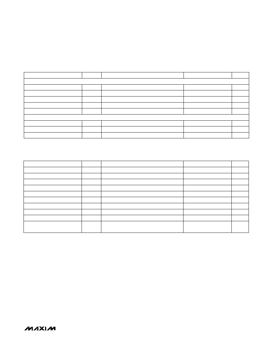
ELECTRICAL CHARACTERISTICS (continued)
(V
DD
= +5V ±5%, V
REF
= +2.5V, V
AGND
= V
DGND
= 0, T
A
= T
MIN
to T
MAX
, unless otherwise noted. Typical values are at T
A
= +25°C.)
TIMING CHARACTERISTICS
(V
DD
= +5V ±5%, V
REF
= +2.5V, V
AGND
= V
DGND
= 0, CMOS inputs, T
A
= T
MIN
to T
MAX
, unless otherwise noted.)
Note 1: Refer to the MAX541 for the 1LSB (max) INL version.
Note 2: Gain error tested at V
REF
= +2.0V, +2.5V, and +3.0V.
Note 3: R
OUT
tolerance is typically ±20%.
Note 4: Min/max ranges guaranteed by gain-error test. Operation outside min/max limits will result in degraded performance.
Note 5: Reference input resistance is code dependent, minimum at 8555 hex.
Note 6: Slew-rate value is measured from 0% to 63%.
Note 7: Guaranteed by design. Not production tested.
V
IN
= 0
(Note 7)
CONDITIONS
mW
1.5
PD
Power Dissipation
mA
0.3
1.1
I
DD
Positive Supply Current
V
4.75
5.25
V
DD
Positive Supply Range
V
0.40
V
H
Hysteresis Voltage
pF
10
C
IN
Input Capacitance
µA
±1
I
IN
Input Current
V
0.8
V
IL
Input Low Voltage
V
2.4
V
IH
Input High Voltage
UNITS
MIN
TYP
MAX
SYMBOL
PARAMETER
(Note 7)
CONDITIONS
µs
20
V
DD
High to CS Low
(power-up delay)
ns
45
t
CL
SCLK Pulse Width Low
ns
45
t
CH
MHz
10
f
CLK
SCLK Frequency
SCLK Pulse Width High
ns
0
t
DH
DIN to SCLK High Hold
ns
40
t
DS
DIN to SCLK High Setup
ns
45
t
CSS0
CS Low to SCLK High Setup
ns
45
t
CSS1
CS High to SCLK High Setup
ns
30
t
CSH0
SCLK High to CS Low Hold
ns
45
t
CSH1
SCLK High to CS High Hold
UNITS
MIN
TYP
MAX
SYMBOL
PARAMETER
STATIC PERFORMANCE—REFERENCE SECTION
STATIC PERFORMANCE—DIGITAL INPUTS
POWER SUPPLY