Table 5. input sampling capacitor vs. gain, Unipolar and bipolar modes – Rainbow Electronics MX7705 User Manual
Page 19
Increasing the gain increases the resolution of the ADC
(LSB size decreases), but reduces the differential input
voltage range. Calculate 1 LSB in unipolar mode using
the following equation:
where V
REF
= V
REF+
- V
REF-.
For a gain of one and V
REF
= 2.5V, the full-scale volt-
age in unipolar mode is 2.5V and 1 LSB
≈ 38.1µV. For a
gain of four, the full-scale voltage in unipolar mode is
0.625V (V
REF
/ GAIN) and 1 LSB
≈ 9.5µV. The differen-
tial input voltage range in this example reduces from
2.5V to 0.625V, and the resolution increases, since the
LSB size decreased from 38.1µV to 9.5µV.
Calculate 1 LSB in bipolar mode using the following
equation:
where V
REF
= V
REF+
- V
REF-.
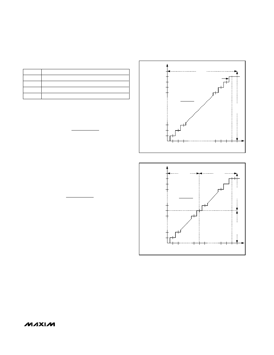
Unipolar and Bipolar Modes
The B/U bit in the setup register (Table 9) configures
the MX7705 for unipolar or bipolar transfer functions.
Figures 4 and 5 illustrate the unipolar and bipolar trans-
fer functions, respectively.
In unipolar mode, the digital output code is straight
binary. When AIN+ = AIN-, the outputs are at zero
scale, which is the lower endpoint of the transfer func-
tion. The full-scale endpoint is given by AIN+ - AIN- =
V
REF
/ GAIN, where V
REF
= V
REF+
- V
REF-
.
In bipolar mode, the digital output code is in offset
binary. Positive full scale is given by AIN+ - AIN- =
+V
REF
/ GAIN and negative full scale is given by AIN+ -
AIN- = -V
REF
/ GAIN. When AIN+ = AIN-, the outputs
are at zero scale, which is the midpoint of the bipolar
transfer function.
When the MX7705 is in buffered mode, the absolute and
common-mode analog input voltage ranges reduce to
between (GND + 50mV) and (V
DD
- 1.5V). The differential
input voltage range is not affected in buffered mode.
1
65 536
2
(
,
)
LSB
V
GAIN
REF
=
×
1
65 536
(
,
)
LSB
V
GAIN
REF
=
MX7705
16-Bit, Low-Power, 2-Channel,
Sigma-Delta ADC
______________________________________________________________________________________
19
Table 5. Input Sampling Capacitor vs. Gain
GAIN
INPUT SAMPLING CAPACITOR (C
SAMP
) (pF)
1
3.75
2
7.5
4
15
8–128
30
0
1
2
3
0000 0000 0000 0000
0000 0000 0000 0001
0000 0000 0000 0010
0000 0000 0000 0011
FULL-SCALE TRANSITION
1 LSB =
V
REF
(GAIN) (65,536)
65,535
65,533
DIFFERENTIAL INPUT VOLTAGE (LSB)
1111 1111 1111 1101
1111 1111 1111 1110
1111 1111 1111 1111
1111 1111 1111 1100
V
REF
/ GAIN
V
REF
/ GAIN
BINAR
Y OUTPUT CODE
Figure 4. MX7705 Unipolar Transfer Function
1 LSB =
V
REF
(GAIN) (65,536)
0
+1
-1
0000 0000 0000 0000
0000 0000 0000 0001
0000 0000 0000 0010
+32,767
BINAR
Y OUTPUT CODE
+32,765
1111 1111 1111 1101
1111 1111 1111 1110
1111 1111 1111 1111
1000 0000 0000 0000
1000 0000 0000 0001
0111 1111 1111 1111
x 2
-32,768
-32,766
DIFFERENTIAL INPUT VOLTAGE (LSB)
V
REF
/ GAIN
V
REF
/ GAIN
V
REF
/ GAIN
V
REF
/ GAIN
Figure 5. MX7705 Bipolar Transfer Function