Absolute maximum ratings, Electrical characteristics – Rainbow Electronics MAX14528 User Manual
Page 2
MAX14527/MAX14528
Adjustable Overvoltage Protector
with High Accuracy
2
_______________________________________________________________________________________
ABSOLUTE MAXIMUM RATINGS
Stresses beyond those listed under “Absolute Maximum Ratings” may cause permanent damage to the device. These are stress ratings only, and functional
operation of the device at these or any other conditions beyond those indicated in the operational sections of the specifications is not implied. Exposure to
absolute maximum rating conditions for extended periods may affect device reliability.
(All voltages referenced to GND.)
IN ............................................................................-0.3V to +30V
OUT .............................................................-0.3V to (V
IN
+ 0.3V)
OVLO........................................................................-0.3V to +6V
Continuous IN Current .............................................................1A
Peak IN Current (Note 1)..........................................................5A
Continuous OVLO Current ...................................................50µA
Continuous Power Dissipation (T
A
= +70°C)
8-Pin TDFN (derate 11.9mW/°C above +70°C) ...........954mW
Package Junction-to-Ambient Thermal Resistance (
θ
JA
)
(Note 2) .....................................................................83.9°C/W
Package Junction-to-Case Thermal Resistance (
θ
JC
)
(Note 2) ........................................................................37°C/W
Operating Temperature Range ...........................-40°C to +85°C
Junction Temperature ......................................................+150°C
Storage Temperature Range .............................-65°C to +150°C
Lead Temperature (soldering) .........................................+300°C
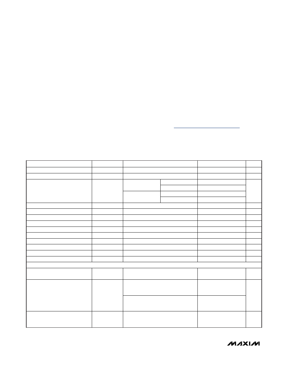
ELECTRICAL CHARACTERISTICS
(V
IN
= +2.2V to +28V, T
A
= -40°C to +85°C, unless otherwise noted. Typical values are at V
IN
= +5.0V and T
A
= +25°C.) (Note 3)
PARAMETER
SYMBOL
CONDITIONS
MIN
TYP
MAX
UNITS
Input Voltage Range
V
IN
2.2
28
V
Input Supply Current
I
IN
V
IN
< OVLO
80
160
µA
MAX14527
5.6
5.75
5.9
V
IN
rising
MAX14528
6.55
6.765
7
MAX14527
5.54
5.84
IN Overvoltage Trip Level
V
IN_OVLO
V
IN
falling
MAX14528
6.5
6.95
V
IN Overvoltage Lockout Hysteresis
V
IN_OVLO_HYS
1
%
OVLO Set Threshold
V
OVLO_THRESH
1.2
1.245
1.29
V
Adjustable OVLO Threshold Range
4
8
V
External OVLO Select Threshold
V
OVLO_SELECT
0.15
0.33
0.5
V
Switch On-Resistance
R
ON
100
200
m
Ω
OVLO Clamp
I
CLAMP
= 10µA
3
4.56
5.5
V
OUT Capacitor
C
OUT
1000
µF
OVLO Input Leakage Current
I
OVLO
V
OVLO_THRESH
= 1.245V
-100
+100
nA
Thermal Shutdown
150
°C
Thermal Shutdown Hysteresis
20
°C
TIMING CHARACTERISTICS (Figure 1)
Debounce Time
t
INDBC
Time from 2.2V < V
IN
< V
IN_OVLO
to
V
OUT
= 10% of V
IN
15
ms
2.2V < V
IN
< V
IN_OVLO
, R
LOAD
= 100
Ω,
C
LOAD
= 100µF; V
OUT
from 10% to
90% of V
IN
0.7
Switch Turn-On Time
t
ON
2.2V < V
IN
< V
IN_OVLO
, R
LOAD
= 100
Ω,
C
LOAD
= 1mF; V
OUT
from 10% to 90%
of V
IN
1.4
ms
Switch Turn-Off Time
t
OFF
V
IN
> V
OVLO_THRESH
to V
OUT
= 80% of
V
IN_OVLO
; R
LOAD
= 1k
Ω, V
IN
rising at
2V/100ns
1.3
3.5
µs
Note 1: Limited by thermal shutdown.
Note 2: Package thermal resistances were obtained using the method described in JEDEC specification JESD51-7, using a four-layer
board. For detailed information on package thermal considerations, refer to
www.maxim-ic.com/thermal-tutorial
.
Note 3: All specifications are 100% production tested at T
A
= +25°C, unless otherwise noted. Specifications are over -40°C to +85°C
and are guaranteed by design.