Detailed description, Pin description – Rainbow Electronics MAX5355 User Manual
Page 9
MAX5354/MAX5355
10-Bit Voltage-Output DACs
in 8-Pin µMAX
_______________________________________________________________________________________
9
_______________Detailed Description
The MAX5354/MAX5355 contain a voltage-output digi-
tal-to-analog converter (DAC) that is easily addressed
using a simple 3-wire serial interface. Each IC includes
a 16-bit shift register, and has a double-buffered input
composed of an input register and a DAC register (see
Functional Diagram
). In addition to the voltage output,
the amplifier’s negative input is available to the user.
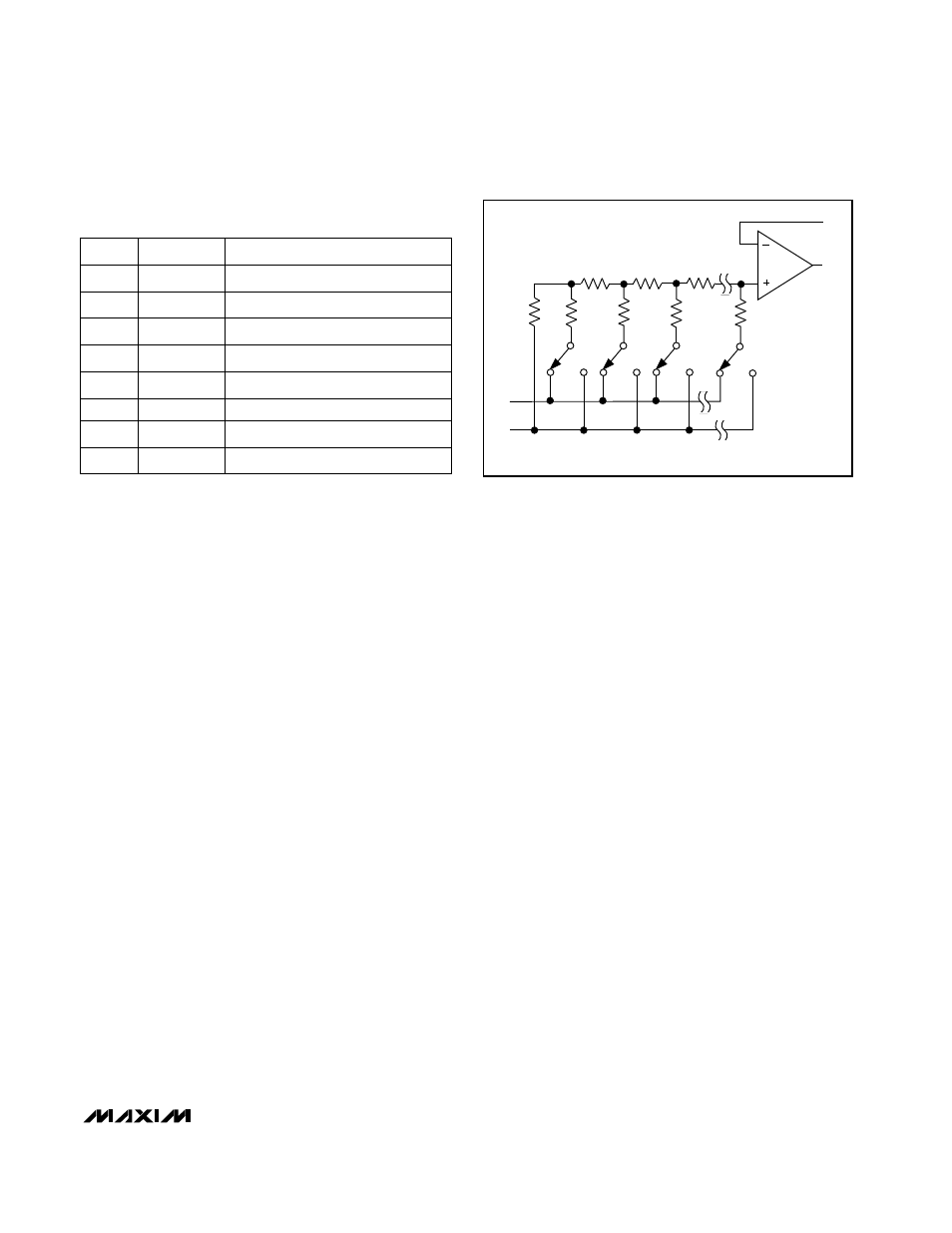
The DAC is an inverted R-2R ladder network that con-
verts a digital input (10 data bits plus three sub-bits)
into an equivalent analog output voltage in proportion
to the applied reference voltage. Figure 1 shows a sim-
plified circuit diagram of the DAC.
Reference Inputs
The reference input accepts positive DC and AC sig-
nals. The voltage at the reference input sets the full-
scale output voltage for the DAC. The reference input
voltage range is 0V to (V
DD
- 1.4V). The output voltage
(V
OUT
) is represented by a digitally programmable volt-
age source, as expressed in the following equation:
V
OUT
= (V
REF
x NB / 1024) x Gain
where NB is the numeric value of the DAC’s binary
input code (0 to 1023), V
REF
is the reference voltage,
and Gain is the externally set voltage gain.
The impedance at the reference input is code depen-
dent, ranging from a low value of 18k
Ω
when the DAC
has an input code of 1550 hex, to a high value exceed-
ing several giga ohms (leakage currents) with an input
code of 0000 hex. Because the input impedance at the
reference pin is code dependent, load regulation of the
reference source is important.
In shutdown mode, the MAX5354/MAX5355’s REF input
enters a high-impedance state with a typical input leak-
age current of 0.001µA.
The reference input capacitance is also code depen-
dent and typically ranges from 15pF (with an input
code of all 0s) to 50pF (at full scale).
The MAX873 +2.5V reference is recommended for use
with the MAX5354.
Output Amplifier
The MAX5354/MAX5355’s DAC output is internally
buffered by a precision amplifier with a typical slew rate
of 0.6V/µs. Access to the output amplifier’s inverting
input provides the user greater flexibility in output gain
setting/signal conditioning (see the
Applications
Information
section).
With a full-scale transition at the MAX5354/MAX5355
output, the typical settling time to ±1/2LSB is 10µs
when loaded with 5k
Ω
in parallel with 100pF (loads less
than 2k
Ω
degrade performance).
The amplifier’s output dynamic responses and settling
performances are shown in the
Typical Operating
Characteristics
.
Shutdown Mode
The MAX5354/MAX5355 feature a software-program-
mable shutdown that reduces supply current to a typical
value of 4µA. Writing 111X XXXX XXXX XXXX as the input-
control word puts the device in shutdown mode (Table 1).
OUT
FB
SHOWN FOR ALL 1s ON DAC
MSB
2R
2R
2R
2R
2R
R
R
R
REF
AGND
Figure 1. Simplified DAC Circuit Diagram
_____________________Pin Description
DAC Output Amplifier Feedback
FB
5
Reference Voltage Input
REF
6
Ground
GND
7
Positive Power Supply
V
DD
8
Serial-Clock Input
SCLK
4
Serial-Data Input
DIN
3
PIN
Chip-Select Input. Active low.
CS
2
DAC Output Voltage
OUT
1
FUNCTION
NAME