Rainbow Electronics MAX5069 User Manual
Page 2
MAX5069
High-Frequency, Current-Mode PWM Controller
with Accurate Oscillator and Dual FET Drivers
2
_______________________________________________________________________________________
ABSOLUTE MAXIMUM RATINGS
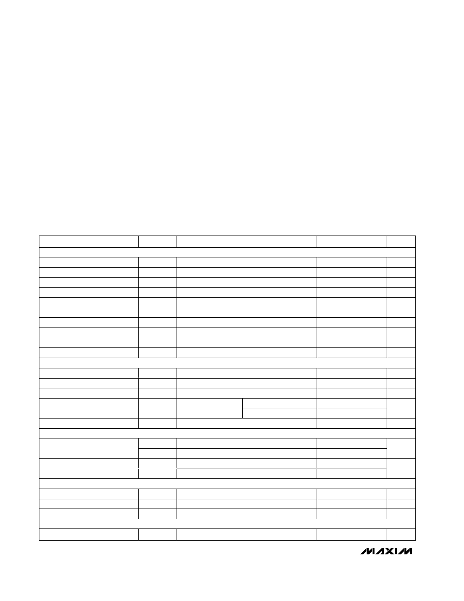
ELECTRICAL CHARACTERISTICS
(V
IN
= +12V for the MAX5069C/D, V
IN
= +23.6V for the MAX5069A/B at startup, then reduces to +12V, C
IN
= C
REG5
= 0.1µF,
C
VCC
= 1µF, R
RT
= 100kΩ, NDRV_ = floating, T
A
= T
MIN
to T
MAX
, unless otherwise noted. Typical values are at T
A
= +25°C.) (Note 1)
Stresses beyond those listed under “Absolute Maximum Ratings” may cause permanent damage to the device. These are stress ratings only, and functional
operation of the device at these or any other conditions beyond those indicated in the operational sections of the specifications is not implied. Exposure to
absolute maximum rating conditions for extended periods may affect device reliability.
IN to PGND ............................................................-0.3V to +30V
IN to AGND.............................................................-0.3V to +30V
V
CC
to PGND..........................................................-0.3V to +13V
V
CC
to AGND..........................................................-0.3V to +13V
FB, COMP, CS, HYST, SYNC, REG5 to AGND ........-0.3V to +6V
UVLO/EN, RT, DT, SCOMP, FLTINT to AGND .........-0.3V to +6V
NDRVA, NDRVB to PGND ..........................-0.3V to (V
CC
+ 0.3V)
AGND to PGND .....................................................-0.3V to +0.3V
Continuous Power Dissipation (T
A
= +70°C)
16-Pin TSSOP-EP (derate 21.3mW/°C above +70°C)...1702mW
Operating Temperature Range..........................-40°C to +125°C
Maximum Junction Temperature .....................................+150°C
Storage Temperature Range .............................-60°C to +150°C
Lead Temperature (soldering, 10s) .................................+300°C
PARAMETER
SYMBOL
CONDITIONS
MIN
TYP
MAX
UNITS
UNDERVOLTAGE LOCKOUT/STARTUP
Bootstrap UVLO Wake-Up Level
V
SUVR
V
IN
rising, MAX5069A/B
19.68
21.6
23.60
V
Bootstrap UVLO Shutdown Level
V
SUVF
V
IN
falling, MAX5069A/B
9.05
9.74
10.43
V
UVLO/EN Wake-Up Threshold
V
ULR2
UVLO/EN rising
1.205
1.230
1.255
V
UVLO/EN Shutdown Threshold
V
ULF2
UVLO/EN falling
1.18
V
HYST FET On-Resistance
R
D S ( ON ) _H
MAX5069B/C only, sinking 50mA,
V
UVLO/EN
= 0V
10
Ω
HYST FET Leakage Current
I
LEAK_H
V
UVLO/EN
= 2V, V
HYST
= 5V
3
nA
IN Supply Current In
Undervoltage Lockout
I
START
V
IN
= +19V, V
UVLO/EN
< V
ULF2
47
90
µA
IN Range
V
IN
10.8
24.0
V
INTERNAL SUPPLIES (V
CC
and REG5)
V
CC
Regulator Set Point
V
CCSP
V
IN
= + 10.8V to + 24V , V
C C
sour ci ng 1µA to 25m A
7.0
10.5
V
REG5 Output Voltage
V
REG5
I
REG5
= 0 to 1mA
4.85
5.00
5.15
V
REG5 Short-Circuit Current Limit
I
REG5_SC
18
mA
f
SW
= 1.25MHz
7
IN Supply Current After Startup
I
IN
V
IN
= +24V
f
SW
= 100kHz
3
mA
Shutdown Supply Current
I
VIN_SD
90
µA
GATE DRIVER (NDRVA, NDRVB)
Z
OUT(LOW)
NDRVA/NDRVB sinking 100mA
2
4
Driver Output Impedance
Z
OUT(HIGH)
NDRVA/NDRVB sourcing 25mA
3
6
Ω
Sinking
1000
Driver Peak Output Current
I
NDRV
Sourcing
650
mA
PWM COMPARATOR
Comparator Offset Voltage
V
OS_PWM
V
COMP
> V
CS
1.30
1.60
2.00
V
Comparator Propagation Delay
t
PD_PWM
V
CS
= 0.1V
40
ns
Minimum On-Time
t
ON(MIN)
Includes t
CS_BLANK
110
ns
CURRENT-LIMIT COMPARATOR
Current-Limit Trip Threshold
V
CS
298
314
330
mV