Rainbow Electronics MAX15032 User Manual
Page 2
MAX15032
500kHz, 36V Output, 600mW PWM
Step-Up DC-DC Converter
2
_______________________________________________________________________________________
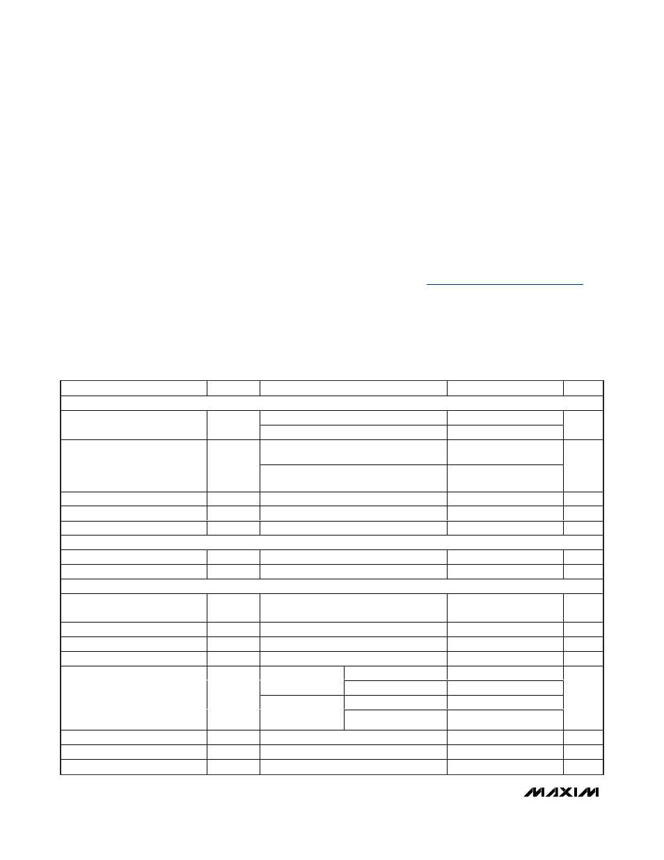
ABSOLUTE MAXIMUM RATINGS
ELECTRICAL CHARACTERISTICS
(V
IN
= +3.3V, V
SHDN
= +3.3V, C
IN
= 10µF, PGND = GND = 0V, T
A
= T
J
= -40°C to +125°C, unless otherwise noted. Typical values
are at T
A
= +25°C. See the
Typical Operating Circuit.) (Note 2)
Stresses beyond those listed under “Absolute Maximum Ratings” may cause permanent damage to the device. These are stress ratings only, and functional
operation of the device at these or any other conditions beyond those indicated in the operational sections of the specifications is not implied. Exposure to
absolute maximum rating conditions for extended periods may affect device reliability.
Note 1: Package thermal resistances were obtained using the method described in JEDEC specification JESD51-7, using a four-
layer board. For detailed information on package thermal considerations, refer to
www.maxim-ic.com/thermal-tutorial.
IN to GND ...............................................................-0.3V to +12V
LX to PGND ............................................................-0.3V to +40V
FB to GND ..............................................................-0.3V to +12V
SHDN to GND..............................................-0.3V to (V
IN
+ 0.3V)
CN to GND .............................................................-0.3V to +12V
CP to GND..............................................................-0.3V to +12V
PGND to GND .......................................................-0.3V to +0.3V
Continuous Power Dissipation (T
A
= +70°C)
8-Pin TDFN (derate 24.4mW/°C above +70°C) ......1951.2mW
Junction-to-Case Thermal Resistance (
θ
JC
) (Note 1) ........8°C/W
Junction-to-Ambient Thermal Resistance (
θ
JA
)
(Note 1) ........................................................................41°C/W
Operating Temperature Range .........................-40°C to +125°C
Junction Temperature ......................................................+150°C
Storage Temperature Range .............................-65°C to +150°C
Lead Temperature (soldering, 10s) .................................+300°C
PARAMETER
SYMBOL
CONDITIONS
MIN
TYP
MAX
UNITS
SUPPLY VOLTAGE
C
CP
= 10nF
2.7
5.5
Supply Voltage Range
V
IN
CP connected to IN
5.5
11
V
V
FB
= 1.4V (no switching), C
CP
= 10nF,
V
IN
= 3.3V
1
2
Supply Current
I
IN
V
FB
= 1.4V (no switching), CP = IN,
V
IN
= 11V
1.5
3
mA
Undervoltage Lockout
V
UVLO
V
IN
rising
2.375
2.5
2.675
V
Undervoltage Lockout Hysteresis
V
UVLO-HYS
100
mV
Shutdown Current
I
SHDN
V
SHDN
= 0V
0.5
µA
LOGIC INPUT (
SHDN)
SHDN Input Low Level
V
IL
0.8
V
SHDN Input High Level
V
IH
2.0
V
BOOST CONVERTER
Output Voltage Adjustment
Range
V
IN
+ 1
36
V
Switching Frequency
f
SW
450
500
550
kHz
FB Set Point
V
FB
1.214
1.245
1.276
V
FB Input Bias Current
I
FB
300
nA
V
IN
= 2.9V, V
CP
= 5.5V
0.42
1
C
CP
= 10nF,
I
LX
= 100mA
V
IN
= 5.5V, V
CP
= 10V
0.33
1
V
IN
= V
CP
= 5.5V
0.42
1
LX Switch On-Resistance
R
DS_ON
CP connected to
IN, I
LX
= 100mA
V
IN
= V
CP
= 11V
0.33
1
Ω
Peak Switch Current Limit
I
LIM_LX
1
1.33
1.7
A
LX Leakage Current
V
LX
= 36V
2
µA
Line Regulation
I
LOAD
= 2mA
0.25
%