Pin description detailed description – Rainbow Electronics MAX8640Z User Manual
Page 5

MAX8640Y/MAX8640Z
500mA, 4MHz/2MHz Synchronous
Step-Down DC-DC Converters in SC70
_______________________________________________________________________________________
5
PIN
NAME
FUNCTION
1
LX
Inductor Connection to the Internal Drains of the p-channel and n-channel MOSFETs. High impedance
during shutdown.
2, 5
GND
Ground. Connect these pins together directly under the IC.
3
OUT
Output Sense Input. Bypass with a ceramic capacitor as close as possible to pin 3 (OUT) and pin 2 (GND).
OUT is internally connected to the internal feedback network.
4
SHDN
Active-Low Shutdown Input. Connect to IN or logic-high for normal operation. Connect to GND or logic-low for
shutdown mode.
6
IN
Supply Voltage Input. Input voltage range is 2.7V to 4.9V. Bypass with a ceramic capacitor as close as
possible to pin 6 (IN) and pin 5 (GND).
Pin Description
Detailed Description
The MAX8640Y/MAX8640Z step-down converters deliv-
er over 500mA to outputs from 0.8V to 2.5V. They utilize
a proprietary hysteretic PWM control scheme that
switches at up to 4MHz (MAX8640Z) or 2MHz
(MAX8640Y), allowing some trade-off between efficien-
cy and size of external components. At loads below
100mA, the MAX8640Y/MAX8640Z automatically switch
to pulse-skipping mode to minimize the typical quies-
cent current (24µA). Output ripple remains low at all
loads, while the skip-mode switching frequency
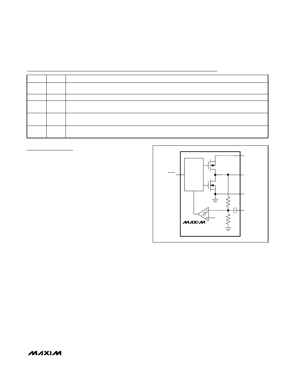
remains ultrasonic down to 1mA (typ) loads. Figure 1 is
the simplified functional diagram.
Control Scheme
A proprietary hysteretic PWM control scheme ensures
high efficiency, fast switching, fast transient response,
low output ripple, and physically tiny external compo-
nents. This control scheme is simple: when the output
voltage is below the regulation threshold, the error
comparator begins a switching cycle by turning on the
high-side switch. This switch remains on until the mini-
mum on-time expires and the output voltage is above
the regulation threshold or the inductor current is above
the current-limit threshold. Once off, the high-side
switch remains off until the minimum off-time expires
and the output voltage falls again below the regulation
threshold. During the off period, the low-side synchro-
nous rectifier turns on and remains on until either the
high-side switch turns on again or the inductor current
approaches zero. The internal synchronous rectifier
eliminates the need for an external Schottky diode.
Voltage-Positioning Load Regulation
The MAX8640Y/MAX8640Z utilize a unique feedback
network. By taking DC feedback from the LX node, the
usual phase lag due to the output capacitor is
removed, making the loop exceedingly stable and
allowing the use of very small ceramic output capacitors.
This configuration yields load regulation equal to the
inductor’s series resistance multiplied by the load current.
This voltage-positioning load regulation greatly reduces
overshoot during load transients, effectively halving the
peak-to-peak output-voltage excursions compared to tra-
ditional step-down converters. See the Load-Transient
Response in the Typical Operating Characteristics.
Shutdown Mode
Connecting SHDN to GND or logic low places the
MAX8640Y/MAX8640Z in shutdown mode and reduces
supply current to 0.1µA (typ). In shutdown, the control
circuitry and internal MOSFET switches turn off and LX
becomes high impedance. Connect SHDN to IN or
logic high for normal operation.
PWM
LOGIC
MAX8640Y
MAX8640Z
GND
LX
IN
SHDN
0.6V
OUT
Figure 1. Simplified Functional Diagram
