Serial programming interface – Rainbow Electronics MAX19505 User Manual
Page 16
MAX19505
Dual-Channel, 8-Bit, 65Msps ADC
16
______________________________________________________________________________________
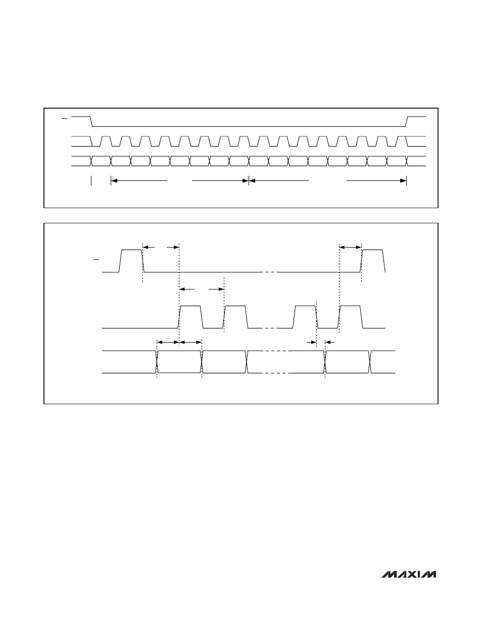
Serial Programming Interface
A serial interface programs the MAX19505 control reg-
isters through the
CS, SDIN, and SCLK inputs. Serial
data is shifted into SDIN on the rising edge of SCLK
when
CS is low. The MAX19505 ignores the data pre-
sented at SDIN and SCLK when
CS is high. C
CS
S must
transition high after each read/write operation. SDIN
also serves as the serial-data output for reading control
registers. The serial interface supports two-byte transfer
in a communication cycle. The first byte is a control
byte, containing the address and read/write instruction,
written to the MAX19505. The second byte is a data
byte and can be written to or read from the MAX19505.
Figure 6 shows a serial-interface communication
cycle. The first SDIN bit clocked in establishes the
communication cycle as either a write or read transac-
tion (0 for write operation and 1 for read operation). The
following 7 bits specify the address of the register to be
written or read. The final 8 SDIN bits are the register
data. All address and data bits are clocked in or out
MSB first. During a read operation, the MAX19505 serial
port drives read data (D7) into SDIN after the falling
edge of SCLK following the 8th rising edge of SCLK.
Since the minimum hold time on SDIN input is zero, the
master can stop driving SDIN any time after the 8th ris-
ing edge of SCLK. Subsequent data bits are driven into
SDIN on the falling edge of SCLK. Output data in a read
operation is latched on the rising edge of SCLK. Figure
7 shows the detailed serial-interface timing diagram.
R/W
A6
A4
A5
A2
A3
A0
A1
D7
D6
D4
D5
D2
D3
D0
D1
R/W
0 = WRITE
1 = READ
CS
SCLK
SDIN
ADDRESS
DATA
WRITE OR READ
CS
t
CSS
t
CSH
t
SDD
t
SDS
t
SDH
t
SCLK
SCLK
SDIN
WRITE
READ
Figure 6. Serial-Interface Communication Cycle
Figure 7. Serial-Interface Timing Diagram