Electrical characteristics (continued) – Rainbow Electronics MAX5940B User Manual
Page 3
MAX5940A/MAX5940B
IEEE 802.3af PD Interface Controller
For Power-Over-Ethernet
_______________________________________________________________________________________
3
Note 1:
All min/max limits are production tested at +85°C. Limits at +25°C and -40°C are guaranteed by design.
Note 2:
The input offset current is illustrated in Figure 1.
Note 3:
Effective differential input resistance is defined as the differential resistance between GND and V
EE
without any external
resistance. See Figure 1.
Note 4: Classification current is turned off whenever the IC is in power mode.
Note 5:
See
Table
2 in the PD Classification Mode section. R
DISC
and R
CL
must be ±1%, 100ppm or better. I
CLASS
includes the IC
bias current and the current drawn by R
DISC
.
Note 6:
See the Thermal Dissipation section for details.
Note 7:
When UVLO is connected to the midpoint of an external resistor-divider with a series resistance of 25.5k
Ω (±1%), the turn-
on threshold set-point for the power mode is defined by the external resistor-divider. Make sure the voltage on the UVLO
pin does not exceed its maximum rating of 8V when V
IN
is at the maximum voltage (MAX5940B only).
Note 8:
When the UVLO input voltage is below V
TH,G,UVLO,
the MAX5940B sets the UVLO threshold internally.
Note 9:
An input voltage or V
UVLO
glitch below their respective thresholds shorter than or equal to t
OFF_DLY
does not cause the
MAX5940A/MAX5940B to exit power-on mode (as long as the input voltage remains above an operable voltage level of 12V).
Note 10: Guaranteed by design.
Note 11: PGOOD references to OUT while PGOOD references to V
EE
.
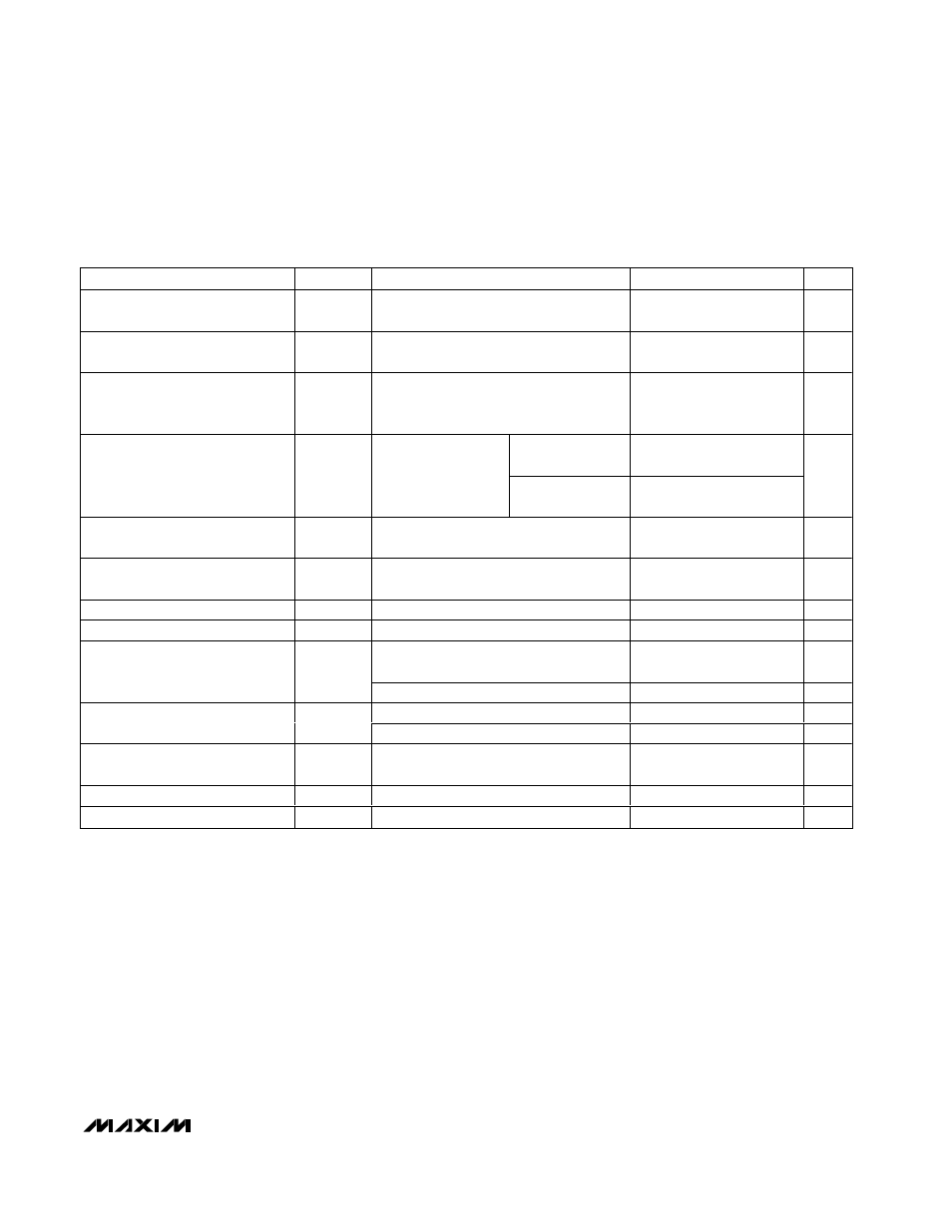
PARAMETER
SYMBOL
CONDITIONS
MIN
TYP
MAX
UNITS
UVLO Input Ground-Sense
Threshold (Note 8)
V
TH,G,UVLO
50
440
mV
UVLO Input Ground-Sense Glitch
Rejection
UVLO = V
EE
7
µs
Power Turn-Off Voltage,
Undervoltage Lockout Deglitch
Time (Note 9)
t
OFF_DLY
V
IN
, V
UVLO
falling
0.32
ms
T
A
= +25°C
(Note 10)
0.6
1.1
Isolation Switch N-Channel
MOSFET On-Resistance
R
ON
Output current =
300mA, V
GATE
= 6V,
measured between
OUT and V
EE
T
A
= +85°C
0.8
1.5
Ω
Isolation Switch N-Channel
MOSFET Off-Threshold Voltage
V
GSTH
OUT = GND, V
GATE
- V
EE,
output current
< 1µA
0.5
V
GATE Pulldown Switch Resistance
R
G
Power-off mode, V
IN
= 12V,
UVLO = V
EE
for MAX5940B
38
80
Ω
GATE Charging Current
I
G
V
GATE
= 2V
5
10
15
µA
GATE High Voltage
V
GATE
I
GATE
= 1µA
5.59
5.76
5.93
V
V
OUT
- V
EE
, |V
OUT
- V
EE
| decreasing,
V
GATE
= 5.75V
1.16
1.23
1.31
V
PGOOD, PGOOD Assertion V
OUT
Threshold
V
OUTEN
Hysteresis
70
mV
(GATE - V
EE
) increasing, OUT = V
EE
4.62
4.76
4.91
V
PGOOD, PGOOD Assertion V
GATE
Threshold
V
GSEN
Hysteresis
80
mV
PGOOD, PGOOD Output Low
Voltage (Note 11)
V
OLDCDC
I
SINK
= 2mA; for PGOOD, OUT
≤
(GND - 5V)
0.4
V
PGOOD Leakage Current (Note 11)
GATE = high, GND - V
OUT
= 67V
1
µA
PGOOD Leakage Current (Note 11)
GATE = V
EE
, PGOOD - V
EE
= 67V
1
µA
ELECTRICAL CHARACTERISTICS (continued)
(V
IN
= (GND - V
EE
) = 48V, GATE = PGOOD = PGOOD = OUT = OPEN, UVLO = V
EE
, T
A
= -40
°C to +85°C, unless otherwise noted.
Typical values are at T
A
= +25
°C. All voltages are referenced to V
EE
, unless otherwise noted.) (Note 1)