Electrical characteristics: max5353 (continued) – Rainbow Electronics MAX5353 User Manual
Page 5
MAX5352/MAX5353
Low-Power, 12-Bit Voltage-Output DACs
with Serial Interface
_______________________________________________________________________________________
5
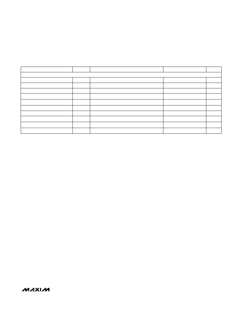
ELECTRICAL CHARACTERISTICS: MAX5353 (continued)
(V
DD
= +3.15V to +3.6V, REF = 1.25V, GND = 0V, R
L
= 5k
Ω
, C
L
= 100pF, T
A
= T
MIN
to T
MAX
, unless otherwise noted. Typical values
are at T
A
= +25°C. Output buffer connected in unity-gain configuration (Figure 8).)
ns
CONDITIONS
40
t
CH
SCLK Pulse Width High
ns
100
t
CP
SCLK Clock Period
ns
40
t
CSS
CS Fall to SCLK Rise Setup Time
ns
40
t
DS
DIN Setup Time
ns
0
t
CSH
SCLK Rise to CS Rise Hold Time
ns
40
t
CL
SCLK Pulse Width Low
UNITS
MIN
TYP
MAX
SYMBOL
PARAMETER
ns
40
t
CS1
CS Rise to SCLK Rise Hold Time
ns
0
t
DH
DIN Hold Time
ns
100
t
CSW
CS Pulse Width High
ns
40
t
CS0
SCLK Rise to CS Fall Delay
Note 4:
Guaranteed from code 22 to code 4095 in unity-gain configuration.
Note 5:
Accuracy is better than 1LSB for V
OUT
= 8mV to V
DD
- 150mV, guaranteed by a power-supply rejection test at the
end points.
Note 6:
R
L
=
∞
, digital inputs at GND or V
DD
.
TIMING CHARACTERISTICS
(Figure 6)