Detailed description, Applications information – Rainbow Electronics MAX9053 User Manual
Page 9

Detailed Description
The MAX9039–MAX9043 and MAX9050–MAX9053 fea-
ture single/dual, low-power, low-voltage comparators
and a precision voltage reference. They operate from a
single 2.5V to 5.5V (MAX9039/MAX904_) or 2.7V to
5.5V (MAX905_) supply. The single comparators with
reference, (MAX9039/MAX9040/MAX9041/MAX9050/
MAX9051 consume only 40µA of supply current, while
the dual comparators with reference (MAX9042/
MAX9043/MAX9052/MAX9053) consume only 55µA of
supply current. Their common-mode input range
extends 0.25V beyond each rail. Internal hysteresis
ensures clean output switching, even with slow-moving
input signals.
The output stage employs a unique design that mini-
mizes supply current surges while switching, virtually
eliminating the supply glitches typical of many other
comparators. Large internal output drivers allow rail-to-
rail output swing that can sink and source up to 8mA of
current.
The precision reference uses a proprietary curvature-
correction circuit and laser-trimmed thin-film resistors,
resulting in a temperature coefficient of less than 30ppm/°C
over the extended temperature range and initial accuracy
of 0.4% (A grade). The reference output voltage is set to
1.23V in the MAX9039, 2.048V in the MAX9040–MAX9043,
and to 2.500V in the MAX9050–MAX9053.
Comparator Input Stage Circuitry
The devices’ input common-mode range extends from
(V
EE
- 0.25V) to (V
CC
+ 0.25V). These comparators may
operate at any differential input voltage within these lim-
its. Input bias current is typically 1.0pA if the input volt-
age is between the supply rails. Comparator inputs are
protected from overvoltage by internal body diodes
connected to the supply rails. As the input voltage
exceeds the supply rails, these body diodes become
forward biased and begin to conduct. Consequently,
bias currents increase exponentially as the input volt-
age exceeds the supply rails.
Comparator Output Stage Circuitry
The comparators in these devices contain a unique
output stage capable of rail-to-rail operation with loads
up to 8mA. Many comparators consume orders-of-mag-
nitude more current during switching than during
steady-state operation. However, with this family of com-
parators, the supply current change during an output
transition is extremely small. The Typical Operating
Characteristics graph Supply Current vs. Switching
Frequency shows the minimal supply current increase
as the output switching frequency approaches 1MHz.
This characteristic reduces the need for power-supply
filter capacitors to reduce glitches created by compara-
tor switching currents. Another advantage realized in
high-speed, battery-powered applications is a substan-
tial increase in battery life.
Applications Information
Additional Hysteresis
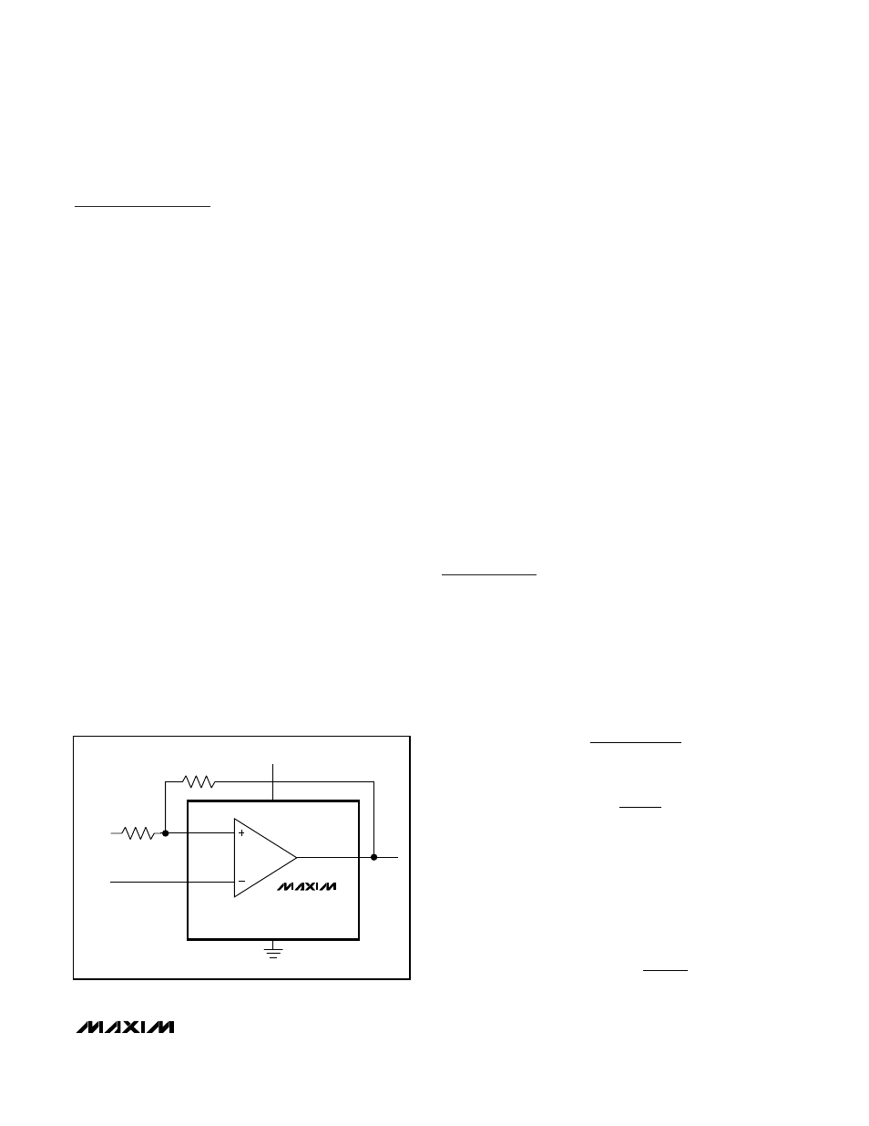
These comparators have ±3mV internal hysteresis.
Additional hysteresis can be generated with two resis-
tors using positive feedback (Figure 1). Use the follow-
ing procedure to calculate resistor values:
1) Calculate the trip points of the comparator using
these formulas:
and
V
TH
is the threshold voltage at which the comparator
switches its output from high to low as V
IN
rises
above the trip point. V
TL
is the threshold voltage at
which the comparator switches its output from low to
high as V
IN
drops below the trip point.
2) The hysteresis band will be:
V
V
R
R
R
TL
REF
=
−
+
1
2
1
2
V
V
V
V
R
R
R
TH
REF
CC
REF
=
+
−
(
)
+
2
1
2
MAX9039–MAX9043/MAX9050–MAX9053
Micropower, Single-Supply, UCSP/SOT23
Comparator + Precision Reference ICs
_______________________________________________________________________________________
9
MAX9039–MAX9043
MAX9050–MAX9053
OUT
IN+
IN-
R2
R1
V
IN
V
REF
V
CC
V
EE
V
CC
Figure 1. Additional Hysteresis
V
V
V
V
R
R
R
HYS
TH
TL
CC
=
−
=
+
2
1
2
