Rainbow Electronics MAX8884Z User Manual
Page 2

MAX8884Y/MAX8884Z
700mA DC-DC Step-Down Converters
with Dual 300mA LDO in 2mm x 2mm CSP
2
_______________________________________________________________________________________
ABSOLUTE MAXIMUM RATINGS
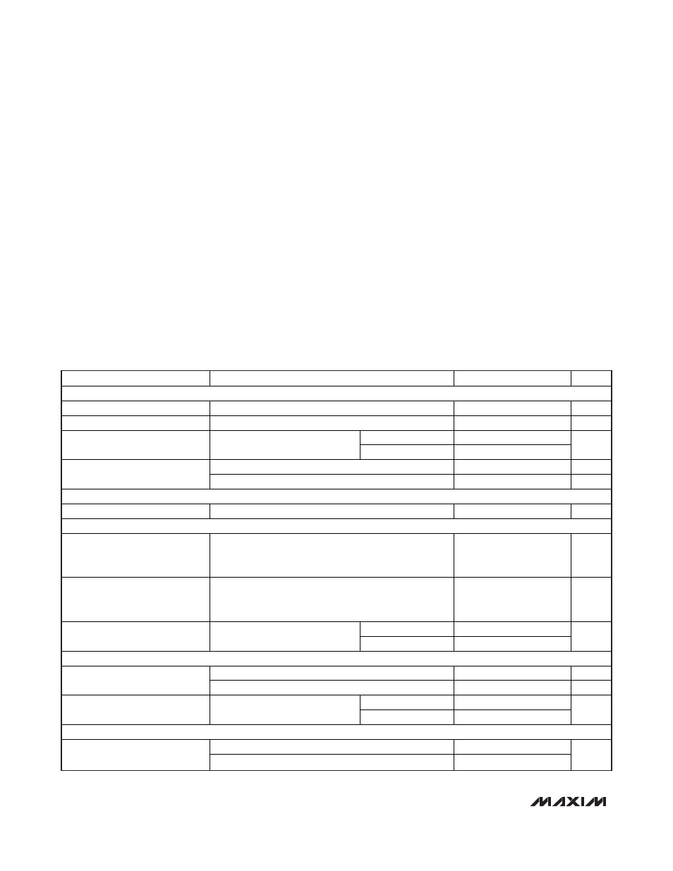
ELECTRICAL CHARACTERISTICS
(V
IN1A
= V
IN1B
= V
IN2
= V
LDO1_EN
= V
LDO2_EN
= V
BUCK_EN
= 3.6V. T
A
= -40°C to +85°C, typical values are at T
A
= +25°C, unless
otherwise noted.) (Note 1)
Stresses beyond those listed under “Absolute Maximum Ratings” may cause permanent damage to the device. These are stress ratings only, and functional
operation of the device at these or any other conditions beyond those indicated in the operational sections of the specifications is not implied. Exposure to
absolute maximum rating conditions for extended periods may affect device reliability.
IN1A, IN1B, IN2, REFBP to AGND ........................-0.3V to +6.0V
FB to PGND ...........................................................-0.3V to +6.0V
SEL, BUCK_EN to AGND...............-0.3V to (V
IN1A
/V
IN1B
+ 0.3V)
LDO1, LDO2, LDO1_EN, LDO2_EN
to AGND.................................................-0.3V to (V
IN2
+ 0.3V)
IN2 to IN1A, IN1B ..................................................-0.3V to +0.3V
AGND to PGND .....................................................-0.3V to +0.3V
IN1A, IN1B, LX Current .....................................................1A
RMS
Continuous Power Dissipation (T
A
= +70°C)
16-Bump CSP (derate 12.5mW/°C above +70°C) ..............1W
Operating Temperature .......................................-40°C to +85°C
Junction Temperature ......................................................+150°C
Storage Temperature Range .............................-65°C to +150°C
Bump Temperature*.........................................................+260°C
PARAMETER
CONDITIONS
MIN
TYP
MAX
UNITS
INPUT SUPPLY
Input Voltage
V
IN1A
, V
IN1B
, V
IN2
2.7
5.5
V
Input Undervoltage Threshold
V
IN1A
, V
IN1B
, V
IN2
rising, 180mV typical hysteresis
2.52
2.63
2.70
V
T
A
= +25°C
0.1
4
Shutdown Supply Current
V
BUCK_EN
= V
LDO1_EN
=
V
LDO2_EN
= 0
T
A
= +85°C
0.1
μA
V
BUCK_EN
= 0, I
LDO1
= I
LDO2
= 0A
140
230
μA
No-Load Supply Current
V
LDO1_EN
= V
LDO2_EN
= 0, I
BUCK
= 0A, no switching
50
80
μA
THERMAL PROTECTION
Thermal Shutdown
T
A
rising, 20°C typical hysteresis
+160
°C
LOGIC CONTROL
Logic Input-High Voltage
(BUCK_EN, SEL, LDO1_EN,
LDO2_EN)
2.7V
V
IN1A
= V
IN1B
= V
IN2
5.5V
1.3
V
Logic Input-Low Voltage
(BUCK_EN, SEL, LDO1_EN,
LDO2_EN)
2.7V
V
IN1A
= V
IN1B
= V
IN2
5.5V
0.4
V
T
A
= +25°C
0.01
1
Logic Input Current (BUCK_EN,
SEL, LDO1_EN, LDO2_EN)
V
IL
= 0 or V
IH
= V
IN1A
= 5.5V
T
A
= +85°C
0.1
μA
FB
SEL = AGND, I
BUCK
= 0A
1.18
1.22
1.24
V
Buck Converter Output Voltage
V
SEL
= V
IN1A
, I
BUCK
= 0A
1.78
1.80
1.85
V
T
A
= +25°C
0.01
1
FB Leakage Current
V
IN1A
= V
IN1B
= V
IN2
= 5.5V,
V
FB
= 0
T
A
= +85°C
1
μA
LX
p-channel MOSFET switch, I
LX
= -40mA
0.18
0.30
On-Resistance
n-channel MOSFET rectifier, I
LX
= 40mA
0.15
0.25
*
These ICs are constructed using a unique set of packaging techniques imposing a limit on the thermal profile used during board level
solder attach and rework. This limit permits only the use of the solder profiles recommended in the industry-standard specification,
JEDEC 020A, paragraph 7.6, Table 3 for IR/VPR and Convection reflow. Preheating is required. Hand or wave soldering is not allowed.
