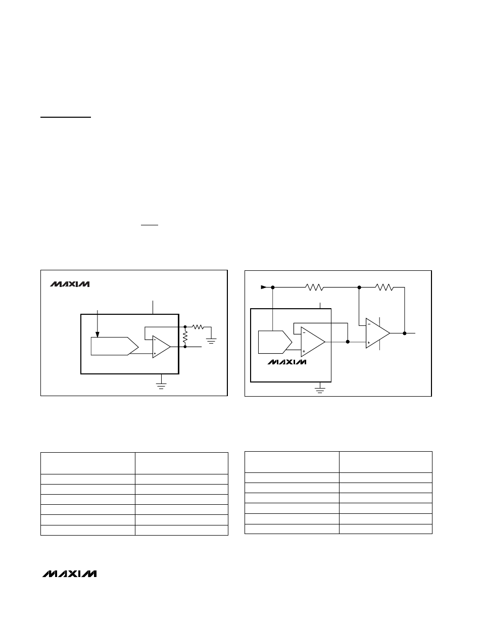
Applications information, Table 2. unipolar code table (circuit of figure 6), Table 3. bipolar code table (circuit of figure 7) – Rainbow Electronics MAX5177 User Manual
Page 13

Applications Information
Unipolar Output
Figure 6 shows the MAX5175/MAX5177 configured for
unipolar, rail-to-rail operation with a gain of +2V/V.
Table 2 lists the codes for unipolar output voltages. The
output voltage is limited to V
DD
.
Bipolar Output
Figure 7 shows the MAX5175/MAX5177 configured for
bipolar output operation. The output voltage is given by
the following equation (FB = OUT):
where N represents the numeric value of the DAC’s
binary input code and V
REF
is the voltage of the exter-
nal reference. Table 3 shows digital codes and the cor-
responding output voltage for Figure 7’s circuit.
Daisy-Chaining Devices
The serial data output pin (DOUT) allows multiple
MAX5175/MAX5177s to be daisy-chained together as
shown in Figure 8. The advantage of this is that only
two lines are needed to control all of the DACs on the
line. The disadvantage is that it takes
n
commands to
program the DACs. Figure 9 shows several MAX5175/
MAX5177s sharing one common DIN signal line. In this
configuration the data bus is common to all devices;
however, more I/O lines are required because each
device needs a dedicated CS line. The advantage of
this configuration is that only one command is needed
to program any DAC.
V
V
2N
4096
1
OUT
REF
=
−
MAX5175/MAX5177
Low-Power, Serial, 12-Bit DACs with
Force/Sense Voltage Output
______________________________________________________________________________________
13
Table 2. Unipolar Code Table (Circuit of
Figure 6)
11 1111 1111 11 (00)
2
·
V
REF
(4095/4096)
10 0000 0000 01 (00)
2
·
V
REF
(2049/4096)
01 1111 1111 11 (00)
10 0000 0000 00 (00)
2
·
V
REF
(2047/4096)
2
·
V
REF
(2048/4096)
00 0000 0000 00 (00)
00 0000 0000 01 (00)
0
2
·
V
REF
(1/4096)
ANALOG OUTPUT
DAC CONTENTS
MSB
LSB
MAX5175
MAX5177
DAC
REF
OUT
10k
10k
GND
+5V/+3.3V
V
DD
FB
Figure 6. Unipolar Output Circuit (Rail-to-Rail)
DAC
V
OUT
V+
V-
+5V/+3.3V
R1 = R2 = 10k
Ω
± 0.1%
MAX5175
MAX5177
REF
10k
10k
FB
OUT
V
DD
GND
Figure 7. Bipolar Output Circuit
Table 3. Bipolar Code Table (Circuit of
Figure 7)
11 1111 1111 11 (00)
ANALOG OUTPUT
+V
REF
[(2
·
4095/4096) - 1]
10 0000 0000 01 (00)
+V
REF
[(2
·
2049/4096) - 1]
01 1111 1111 11 (00)
10 0000 0000 00 (00)
+V
REF
[(2
·
2047/4096) - 1]
+V
REF
[(2
·
2048/4096) - 1]
DAC CONTENTS
MSB
LSB
00 0000 0000 00 (00)
00 0000 0000 01 (00)
-V
REF
+V
REF
[(2
·
1/4096) - 1]
