Texas Instruments SLVP089 User Manual
Page 25

Design Procedures
2-7
Design Procedure
Calculating the pulse-width-modulator gain as the change in output voltage
divided by the change in PWM input voltage gives:
A
PWM
+
D
V
O
D
V
COMP
+
9 – 0
1.3 – 0.65
+
13.85
å
22.8 db
The LC filter has a double pole at:
1
2
p
LC
Ǹ
+
1
2
p
21.6
m
H
168
m
F
Ǹ
+
2.64 kHz
(worst case values) and rolls off at 40-dB per decade after that until the ESR
zero is reached at:
1
2
p
RC
+
1
2
p
(0.025)
ǒ
210
10
–6
Ǔ
+
38 kHz
This information is enough to calculate the required compensation values.
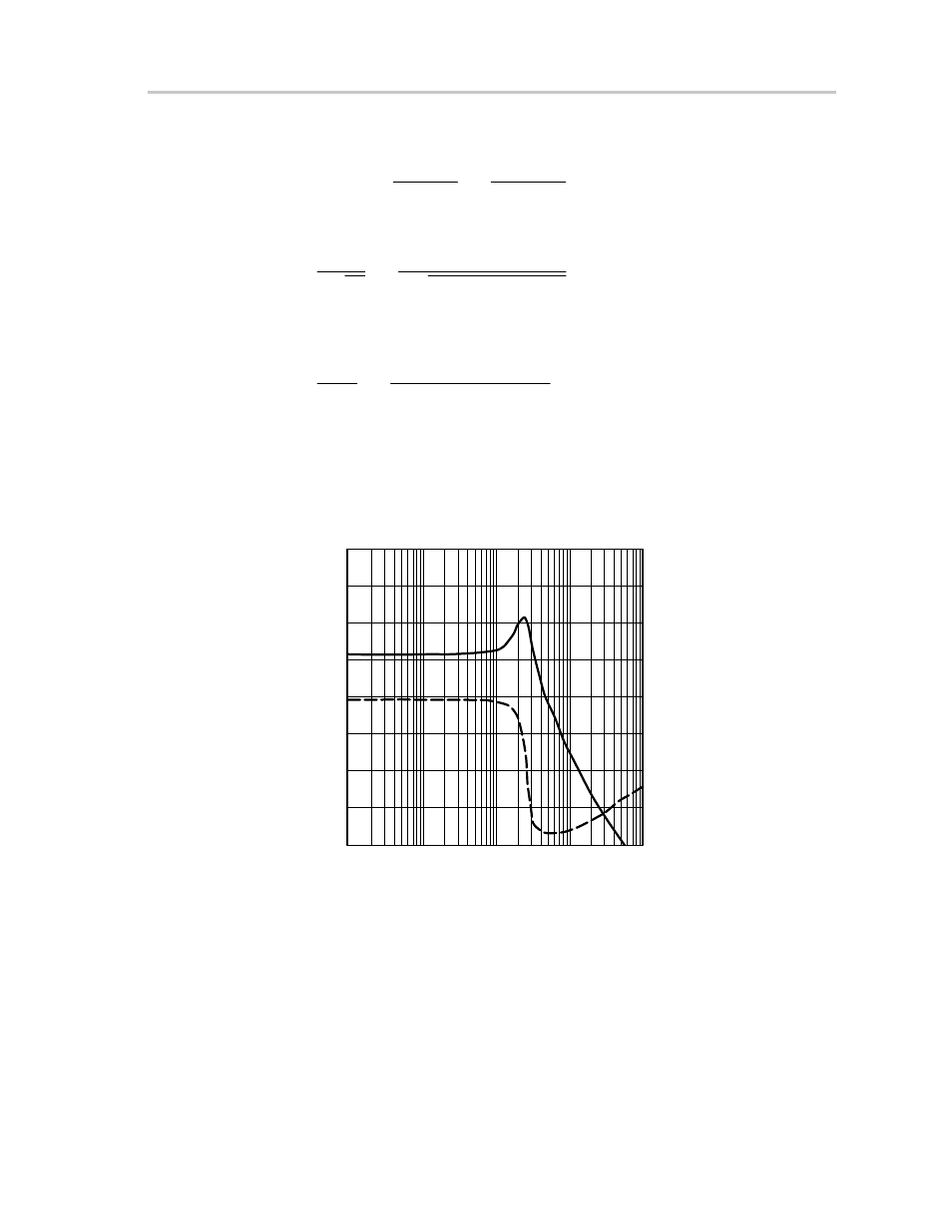
Figure 2–1 shows the power stage gain and phase plots.
Figure 2–1. Power Stage Bode Plot
10
0
–20
–30
Gain
–
Solid
20
40
Frequency
FREQUENCY RESPONSE
50
30
–10
0
–45
–90
–135
–180
–225
–270
–315
–360
Phase
–
Dashed
10
102
103
104
105
This response must be corrected by addition of the following:
-
A pole at zero to give high dc gain
-
Two zeroes at approximately 2.6 kHz to cancel the LC poles
-
A pole at approximately 38 kHz to cancel the ESR zero
-
A final pole to roll off high-frequency gain
The compensation circuit shown in figure 2–2 can be used to implement the
above conditions.
