TDK 73M2901/5V User Manual
Page 3
73M2901/5V
Advanced Single
Chip Modem
3
RESET
A reset is accomplished by holding the RESET pin
high. To ensure a proper power-on reset, the reset
pin must be held high for a minimum of 3
m
s. At
power on, the voltage at VPD, VPA, and RESET
must come up at the same time for a proper reset.
ASYNCHRONOUS AND SYNCHRONOUS SERIAL
DATA INTERFACE
The serial data interface consists of the TXD and
RXD data paths (LSBit shifted in and out first,
respectively); and the TXCLK and RXCLK serial
clock outputs associated with the data pins;
CTS/RTS flow control; DCR, DSR and DTR. In
synchronous mode, the data is passed at the bit rate
(tolerance is +1%, -2.5%).
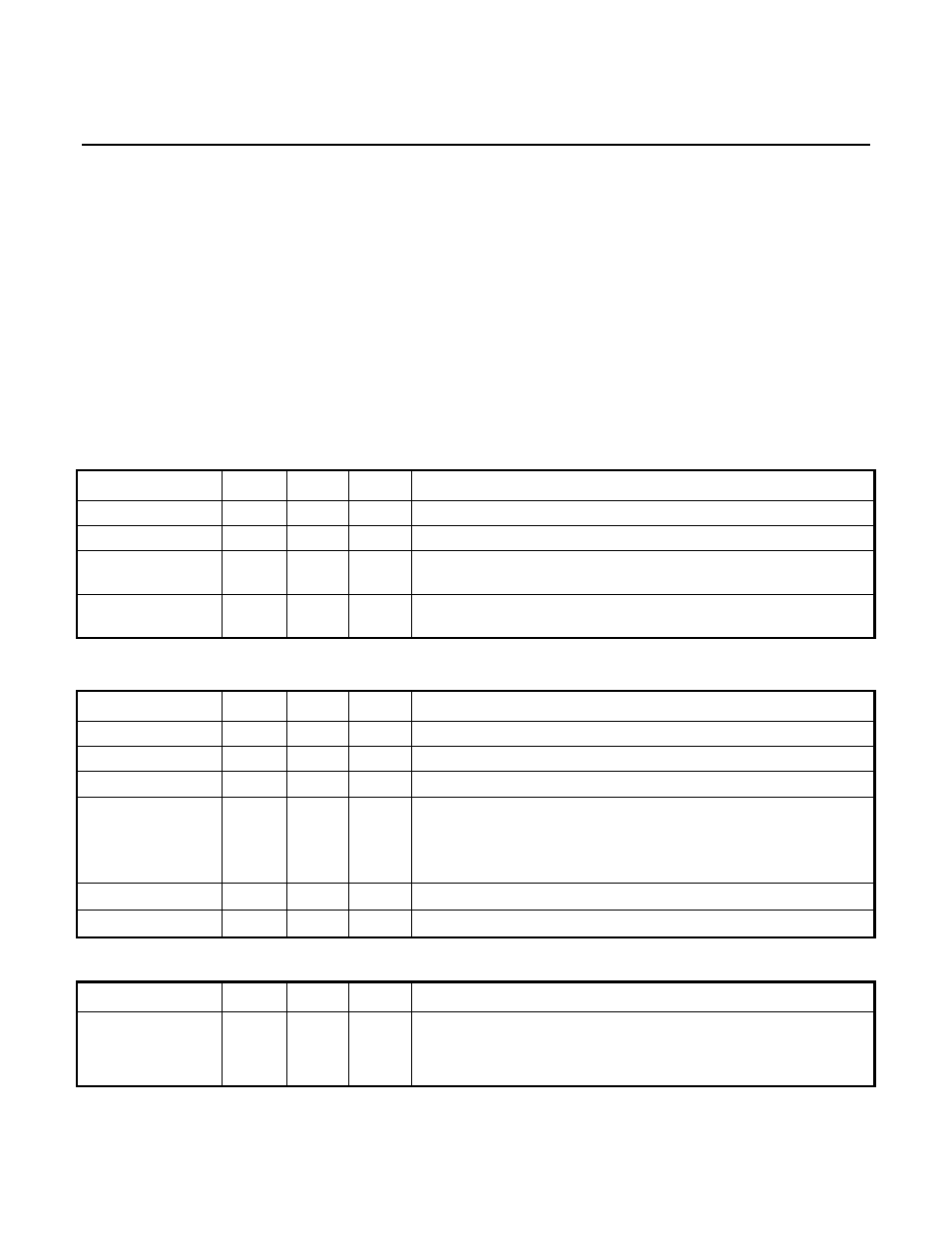
PIN DESCRIPTIONS
POWER PIN DESCRIPTION
PIN NAME
32-PIN 44-PIN TYPE DESCRIPTION
VPA
15
16
I
Positive analog voltage (+ Analog Supply)
VNA
21
22
I
Negative analog voltage. (Analog Ground)
VPD
6, 25,
29
2,12,
27, 33
I
Positive digital voltage (+ Digital Supply)
VND
5, 22,
26
11, 24,
44, 28
I
Negative digital voltage. (Digital Ground)
ANALOG INTERFACE PIN DESCRIPTION
PIN NAME
32-PIN 44-PIN TYPE DESCRIPTION
RXA
20
21
I
Receive analog data
TXAN
16
17
O
Transmit Analog -
TXAP
17
18
O
Transmit Analog +
HBDEN
14
15
I
2w/4w hybrid driver enable pin
0 = Driver configured for 50k
W
or greater load (Tie to VND)
1 = Driver configured for driving line-coupling transformer (Tie to
VPD)
VBG
19
20
O
Analog Band Gap voltage reference pin (0.1
m
F to VNA)
VREF
18
19
O
Analog reference voltage pin (0.1
m
F to VNA)
EXTERNAL INTERRUPTS PIN DESCRIPTIONS
PIN NAME
32-PIN 44-PIN TYPE DESCRIPTION
RING
ASRCH
DTR
2
1
32
39
38
37
I
I
I
External interrupt – Line interface ring detection circuitry input
External interrupt – Autobaud detection, connected to TXD
External interrupt – DTE DTR signal input