Omega Vehicle Security OME-PIO-D56 User Manual
User’s guide
www.omega.com
e-mail: [email protected]
User’s Guide
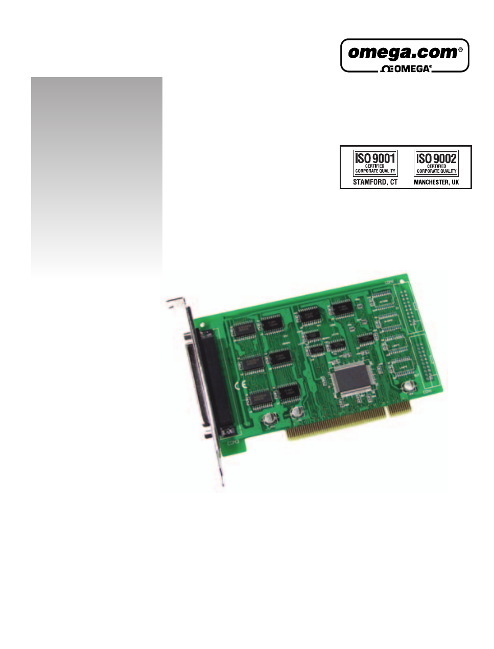
OME-PIO-D56/D24
PCI-Bus
Digital I/O Board
Hardware Manual
Shop online at
Table of contents
Document Outline
- 1. Introduction
- 1.1 Features
- 1.2 Specifications
- 1.3 Order Description
- 1.3.1 Options
- 1.4 PCI Data Acquisition Family
- 1.5 Product Checklist
- 2. Hardware configuration
- 2.1 Board Layout
- 2.2 I/O Port Location
- 2.3 Enabling I/O Operation
- 2.3.1 DI/DO Port Architecture (CON3)
- 2.3.2 DI Port Architecture (CON2)
- 2.3.3 DO Port Architecture (CON1)
- 2.4 Interrupt Operation
- 2.4.1 Interrupt Block Diagram of OME-PIO-D56/D24
- 2.4.2 INT_CHAN_0/1/2/3
- 2.4.3 Initial_high, active_low Interrupt source
- 2.4.4 Initial_low, active_high Interrupt source
- 2.4.5 Muliti-Interrupt Source
- 2.5 Daughter Boards
- 2.5.1 OME-DB-37
- 2.5.2 OME-DN-37
- 2.5.3 OME-DB-8125
- 2.5.4 OME-ADP-20/PCI
- 2.5.5 OME-DB-24PD Isolated Input Board
- 2.5.6 OME-DB-24RD Relay Board
- 2.5.7 OME-DB-24PRD, OME-DB-24POR, OME-DB-24C
- 2.5.8 Daughter Board Comparison Table
- 2.6 Pin Assignment
- 3. I/O Control Register
- 3.1 How to Find the I/O Address
- 3.1.1 PIO_DriverInit
- 3.1.2 PIO_GetConfigAddressSpace
- 3.1.3 Show_PIO_PISO
- 3.2 The Assignment of I/O Address
- 3.3 The I/O Address Map
- 3.3.1 RESET\ Control Register
- 3.3.2 AUX Control Register
- 3.3.3 AUX data Register
- 3.3.4 INT Mask Control Register
- 3.3.5 Aux Status Register
- 3.3.6 Interrupt Polarity Control Register
- 3.3.7 I/O Selection Control Register
- 3.3.8 Read/Write 8-bit data Register
- 3.1 How to Find the I/O Address
- 4. Demo program
- 4.1 PIO_PISO
- 4.1.1 PIO_PISO.EXE for Windows
- 4.2 DEMO1
- 4.3 DEMO2
- 4.4 DEMO3
- 4.5 DEMO4
- 4.6 DEMO5
- 4.1 PIO_PISO
- OME-PIO-D24HW.pdf