Hardware interface, 1 connectors, 2 pin assignment of connector – Rikaline GPS-20 User Manual
Page 6: Rikaline
GPS-20 Operating Manual
Rikaline
Rikaline
Marketing Corp.
5F-1, 125, Roosevelt Road, Sec. 5, Taipei, Taiwan 116
Tel: ++886 2 2934 5456 Fax: ++886 2 2934 4373 E-Mail:
web:
www.rikaline.com.tw
6
3. Hardware interface
3.1 Connectors
3.1.1 Antenna Connector
MCX, RSMA
3.1.2 Interface Connector
20-Pin and 10-Pin straight header, 2mm pitch
3.2 Pin Assignment of Connector
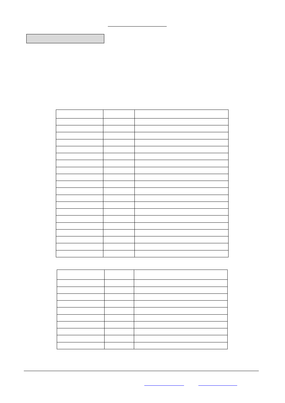
Table 1-1 Pin list of the 20-Pin Digital Interface Connector (CN1)
Pin Number
Name
Description
1
ANT_PWR
Antenna DC Voltage
2
VCC_5V
+5 DC Power Input
3 BAT
Backup
Battery
4
VCC_3V
+3.3V DC Power Input
5
PBRES
Push Button Reset Input. Active Low
6
GPIOA
SW dependent functions (note 1)
7
GPIOB
SW dependent functions (note 1)
8
GPIOC
SW dependent functions (note 1)
9
GPIOD
SW dependent functions (note 1)
10 GND
Ground
11
TXA
Serial Data Output A
12
RXA
Serial Data Input A
13 GND
Ground
14
TXB
Serial Data Output B
15
RXB
Serial Data Input B
16 GND
Ground
17
BOOTSEL
Booting Mode Select
18 GND
Ground
19
TIMEMARK
1PPS Time Mark Output
20 ALT/GPIOE
Alternative
output
(Reserved)
Pin Number
Name
Description
1
GPIOF
SW dependent functions (note 1)
2
JTDI
JTAG software debug function
3
GPIOG
SW dependent functions (note 1)
4
JTMS
JTAG software debug function
5
GPIOH
SW dependent functions (note 1)
6
JTCK
JTAG software debug function
7
GPIOI
SW dependent functions (note 1)
8
JTDO
JTAG software debug function
9
JTRST
JTAG software debug function
Note: 1) Pulled high (VCC/VDD) through on-board 100K Ohm resister.