2 hardware design, Ardware, Esign – Renesas H8S User Manual
Page 15
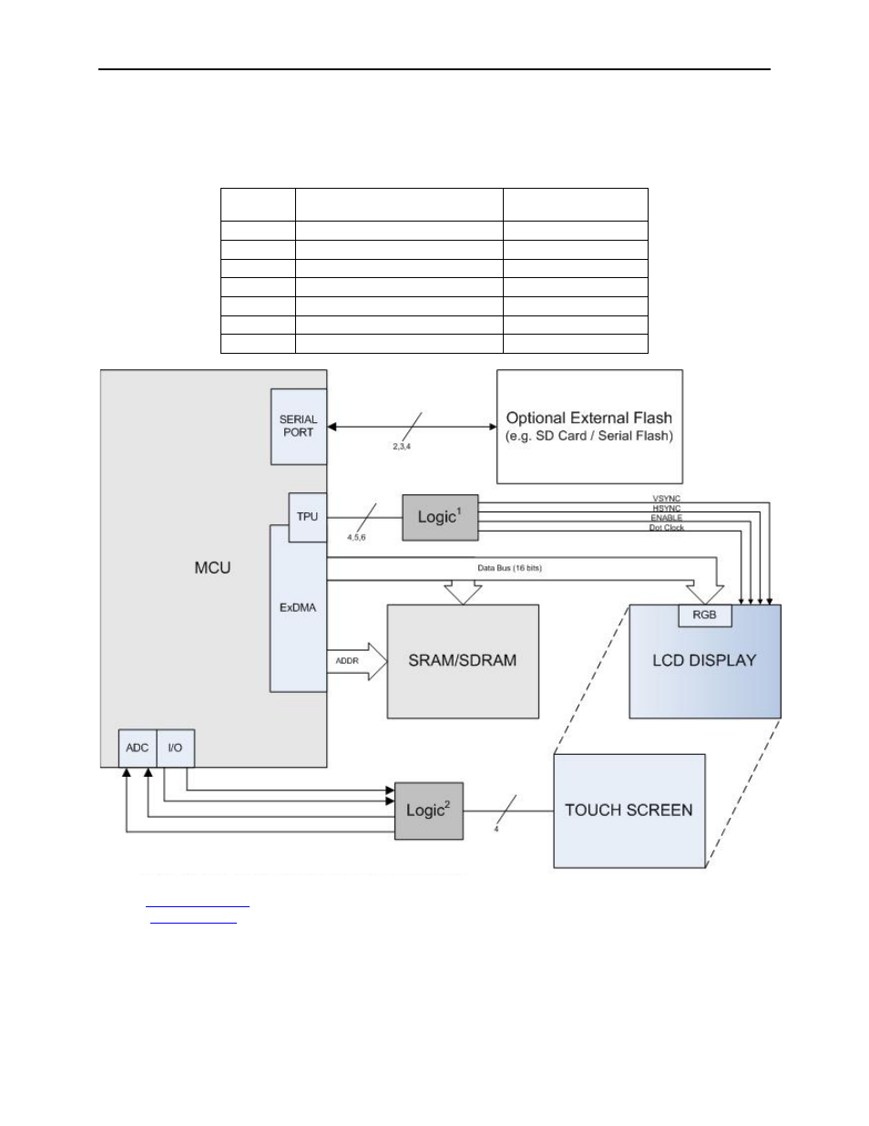
Direct Drive LCD Design Guide
3.2 Hardware
Design
Below is a block diagram of a LCD system which uses Flash and SRAM for respectively storing and
buffering the images to be displayed.
The following table describes the TPU channels and pins used for direct drive. Note that the TPU
synchronization capability is used to create a common time base between the HDEN, HSYNC and
VSYNC pins.
Signal
TPU Channel Requirements
Suggested
Channel
DOTCLK Output using PWM 1 Mode
1, 2, 4 or 5
DOTPER TGR to set period of DOTCLK
same as DOTCLK
HDEN
Output using PWM 2 Mode
1, 2, 4 or 5
HDEN2
TGR for PWM 2 Mode
same as HDEN
HSYNC
Output using PWM 1 Mode
0 or 3
VSYNC
Output using PWM 1 Mode
same as HSYNC
HPER
TGR to set horizontal period
same as HSYNC
Figure 9 Block Diagram
Note 2:
14