LG GSA-4167B User Manual
Page 63
67
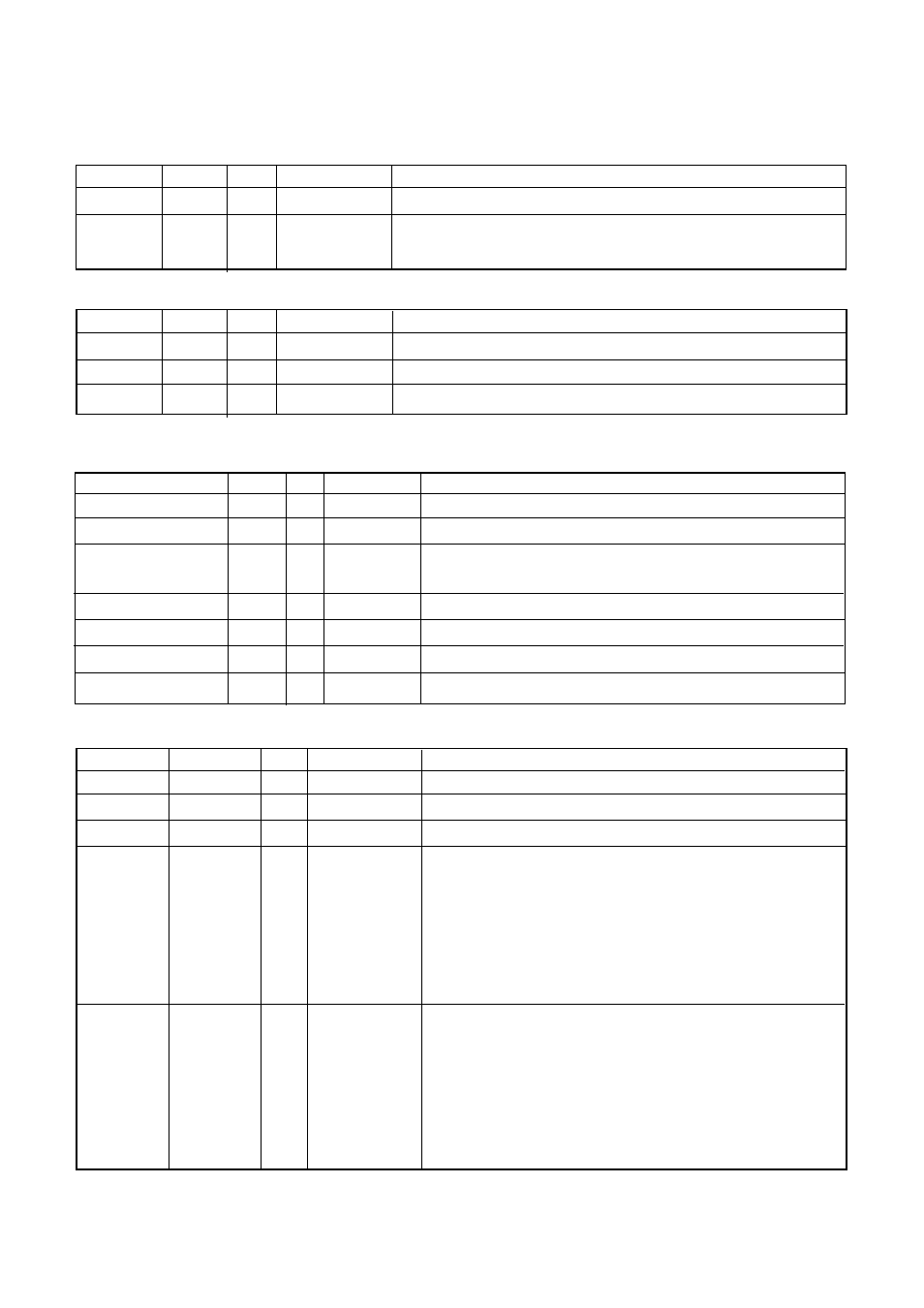
Audio Interface Pin List
Pin Name Pin No.
I/O
destination
Function
DOUT
109
IO
ATAPI
Digital output pin,also functions as the CPU general port 1-2
ROUT
98
AO
ATAPI
Audio Lch & Rch output
LOUT
100
Clock Generator Pin List
Pin Name Pin No.
I/O
destination
Function
FEMCK
119
O
AFE
Front End LSI clock
XCO
106
O
X’tal
Crystal oscillation 33.8688MHz
XCI
107
I
X’tal
Crystal oscillation 33.8688MHz
Flash/SRAM Pin List
Pin Name
Pin No.
I/O
destination
Function
UCS0B
15
O
Flash
H8S / CS0
CPWRB
40
O
Flash / SRAM
H8S / WRB
CPRDB
14
O
Flash / SRAM
H8S / RDB
A[20:1]
39,43,44,
O
Flash / SRAM
H8S / A[20:1]
215,29,30,
33,34,35,
36,37,38,
45,46,47,
48,49,50,
55,16
CPU[15:1]
216,3,4,
IO
Flash / SRAM
H8S / D[15:0]
5,9,10,
CPU[0] can also function as the CPU general port 0-4
(multiplexed).
12,13,25,
24,23,21,
20,19,18
17
H8S Micro-Processor Pin List
CPU
Pin Name
Pin No. I/O
destination
Function
ICUIN7(ACTFLG)
205
IU
DRVR
CPU interrupt port INT7: Pick up protect flag
ICUIN6(EJECTSW)
206
I
Eject Switch CPU interrupt port INT6: EJECTSW interrupt request
ICUIN8(LOADIN)
207
IO
Load Switch CPU general port1-1 also connected to the CPU interrupt
port INT8: Loader in sensor
GPIO07(HEATRUN)
96
5IO
ATAPI
CPU general port 0-7 :Off heat run test input
GPIO06(CSEL)
97
5IO
ATAPI
CPU general port 0-6 ATAPI CSEL
GPIO04(A0)
208
IO
SRAM
CPU general port 0-4, also functions as H8S / A0
GPIO05(UCS1B)
56
IO
SRAM
CPU general port 0-5, also functions as H8S / CS1