Figure 41 sho, Si53xx-rm, Driver receiver – Silicon Laboratories SI5375 User Manual
Page 95
Si53xx-RM
Rev. 1.2
95
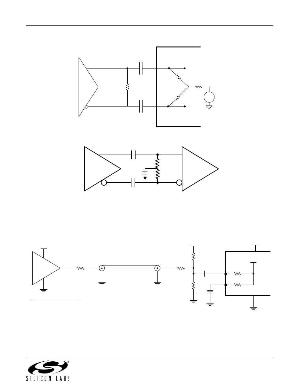
Figure 39. CML/LVDS Termination (1.8, 2.5, 3.3 V)
Figure 40. Center Tap Bypassed Termination
Figure 40 is recommended over a single 100
resistor whenever greater reduction of common-mode noise is
desired. It can be used with any differential termination, either input or output.
Figure 41. CMOS Termination (1.8, 2.5, 3.3 V)
40 k
C
C
±
CKIN
_
CKIN +
V
ICM
300
100
Si53xx
CML/
LVDS
Driver
40 k
Driver
Receiver
50
50
V
DD
V
DD
V
DD
CMOS Driver
R1
33 ohms
50
R2
See Table
R3
150 ohms
C1
100 nF
R4
150 ohms
C2
100 nF
V
ICM
CKIN+
CKIN–
R5 40 kohm
R6 40 kohm
V
DD
R2 Notes
3.3 V 100 ohm Locate R1 near CMOS driver
2.5 V 49.9 ohm Locate other components near Si5317
1.8 V 14.7 ohm Recalculate resistor values for other drive strengths
Additional Notes:
1. Attenuation circuit limits overshoot and undershoot.
2. Use only with ~50% duty cycle clock signals.
3. Assumes the CMOS output can drive 8 mA.
Si53xx