To figure 24 na, Table 26 a, Table 27 for – Silicon Laboratories SI5375 User Manual
Page 65: Si53xx-rm, Table 27. dividers and limits
Si53xx-RM
Rev. 1.2
65
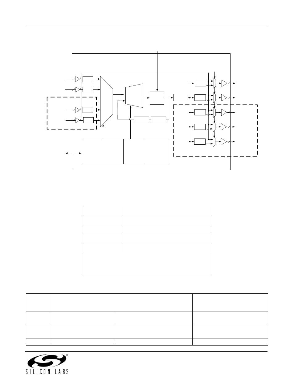
Figure 24. Narrowband PLL Divider Settings
(Si5319, Si5324, Si5326, Si5327, Si5328, Si5368, Si5369, Si5374, Si5375, and Si5376)
Table 26. Narrowband Frequency Limits
Signal
Frequency Limits
CKINn
2 kHz–710 MHz
f
3
2 kHz–2 MHz
f
OSC
4.85–5.67 GHz
f
OUT
2 kHz–1.475 GHz
Note: Fmax = 346 MHz for the Si5328 and 808 MHz for the
Si5327, Si5374, Si5375, and Si5376. Each entry has
500 ppm margins at both ends. The Si5374, Si5375, and
Si5376 have an extend Fosc range of from 4.6 to 6 GHz.
Table 27. Dividers and Limits
Divider
Equation
Si5325, Si5367
Si5319, Si5324, Si5326, Si5327,
Si5328, Si5368, Si5369, Si5374,
Si5375, Si5376
N1
N1 = N1_HS x NCn_LS
N1_HS = [4, 5, …, 11]
NCn_LS = [1, 2, 4, 6, …, 2
20
]
N1_HS = [4, 5, …, 11]
NCn_LS = [1, 2, 4, 6, …, 2
20
]
N2
N2 = N2_HS x N2_LS
N2_HS = 1
N2_LS = [32, 34, 36, …, 2
9
]
N2_HS = [4, 5, …, 11]
N2_LS = [2, 4, 6, …, 2
20
]
N3
N3 = N3n
N3n = [1,2,3,..,2
19
]
N3n = [1,2,3,..,2
19
]
CKIN_1+
CKIN_1–
CKIN_2+
CKIN_2–
CKIN_3+
CKIN_3–
CKIN_4+
CKIN_4–
CKOUT_1+
CKOUT_1–
÷ NC1
1
0
CKOUT_2+
CKOUT_2–
÷ NC2
1
0
CKOUT_3+
CKOUT_3–
÷ NC3
1
0
CKOUT_4+
CKOUT_4–
÷ NC4
1
0
2
2
2
2
2
2
2
2
DCO
f
OSC
Xtal, or Refclock
(Si5319, Si5324, Si5326, Si5327, Si5368, Si5369;
Refclock only for the Si5374, Si5375, and Si5376)
f
x
M
f
3
Digital
Phase
Detector/
Loop Filter
BYPASS
f
3
SPI/I
2
C
Si5319, Si5326,
Si5368
Control
÷ N32
÷ N31
Si5368
Si5368
Note: See section 6.7
for FSYNC details.
÷ N1_HS
CKOUT_5+
CKOUT_5–
÷ NC5
1
0
2
÷ N33
÷ N34
Note: There are multiple outputs at different frequencies because of limitations caused by the DCO and N1_HS.
÷ N2_LS
÷ N2_HS
Bandwidth
Control
FSYNC
(Si5368)
Si5369
Si5369